Method of manufacturing multilayer wiring board

a manufacturing method and technology for wiring boards, applied in printed circuit aspects, conductive pattern formation, chemistry apparatus and processes, etc., can solve the problems of reducing the yield of a product, and the final result of multi-layer wiring boards being judged as “defective”, so as to improve yield, reduce manufacturing time, and achieve high-density wiring

Inactive Publication Date: 2009-12-01
SHINKO ELECTRIC IND CO LTD
View PDF5 Cites 18 Cited by
  • Summary
  • Abstract
  • Description
  • Claims
  • Application Information

AI Technical Summary

Benefits of technology

[0011]An object of the present invention is to provide a method of manufacturing a multilayer wiring board, which achieves a reduction in time period for manufacture and an improvement in yield and enables high-density wiring, and also enables preventing occurrence of misalignment on the occasion of stacking.
[0012]To attain the above object, according to the present invention, there is provided a method of manufacturing a multilayer wiring board, including the steps of: fabricating a first wiring board including an insulating base member, wiring layers formed in desired shapes on both sides of the insulating base member, a conductive post formed on the wiring layer on one surface of the insulating base member, and a first stopper layer formed at a desired position around the conductive post, the first stopper layer having such a predetermined shape as may suppress in-plane misalignment that can possibly occur on the occasion of stacking; fabricating a second wiring board including an insulating base member, wiring layers formed in desired shapes on both sides of the insulating base member, a through hole for insertion of the conductive post therethrough, a connection terminal formed on the wiring layer on one surface of the insulating base member, and a second stopper layer that engages the first stopper layer and functions to suppress the in-plane misalignment on the occasion of the stacking; fabricating a third wiring board including an insulating base member, wiring layers formed in desired shapes on both sides of the insulating base member, and a connection terminal formed on the wiring layer on one surface of the insulating base member; stacking up the first, second and third wiring boards, the respective wiring boards being aligned with one another so that the wiring layers thereof are interconnected via the conductive post and the connection terminals, to thereby provide electrical connections through the wiring boards; and filling resin into a gap between adjacent two of the stacked wiring boards.
[0013]According to the method of manufacturing a multilayer wiring board according to the present invention, the first, second and third wiring boards are fabricated at separate steps. Then, the wiring boards are superposed one on top of another and connected to one another. Thereafter, the resin is filled into the gaps between the wiring boards, whereby a multilayer wiring structure is formed. Accordingly, the method of the present invention can greatly reduce a time period required for manufacture, as compared with the conventional multilayer wiring formation technique using the build-up process.
[0015]The conventional multilayer wiring formation technique using the build-up process uses a laser-based hole formation process for via hole formation and hence requires provision of a land of appropriate size around the via hole opening. This in turn becomes a factor responsible for hindrance to fine-diameter formation or pitch reduction, and hence forms a bottleneck in high-density wiring. As opposed to this, the method of the present invention makes it possible to contribute to achievement of high-density wiring. This is because using the conductive post (e.g., a copper (Cu) post) as the interboard connection terminal makes it adaptable to the fine-diameter formation and the pitch reduction.
[0016]Moreover, the first wiring board is provided with the first stopper layer formed in the predetermined shape at the desired position around the conductive post, and the second wiring board having the through hole for insertion of the conductive post therethrough is also provided with the second stopper layer. Thereby, when the wiring boards are vertically stacked on, the respective stopper layers can engage each other so as to suppress the in-plane misalignment. This makes it possible to prevent the wiring layers of the second wiring board exposed from inner walls of the through holes from coming into electrical contact with sidewalls of the conductive posts.

Problems solved by technology

The conventional manufacturing method using the build-up process has a problem of causing a reduction in the yield of a product (namely, the multilayer wiring board).
This is because, even if a defective condition is encountered at one of all steps, the multilayer wiring board finally obtained is judged as a “defective,” the shipment of which is not permitted.

Method used


Image

  • Method of manufacturing multilayer wiring board
  • Method of manufacturing multilayer wiring board
  • Method of manufacturing multilayer wiring board

Examples


Embodiment Construction

[0024]Description will be given below with regard to preferred embodiments of the present invention with reference to the accompanying drawings.

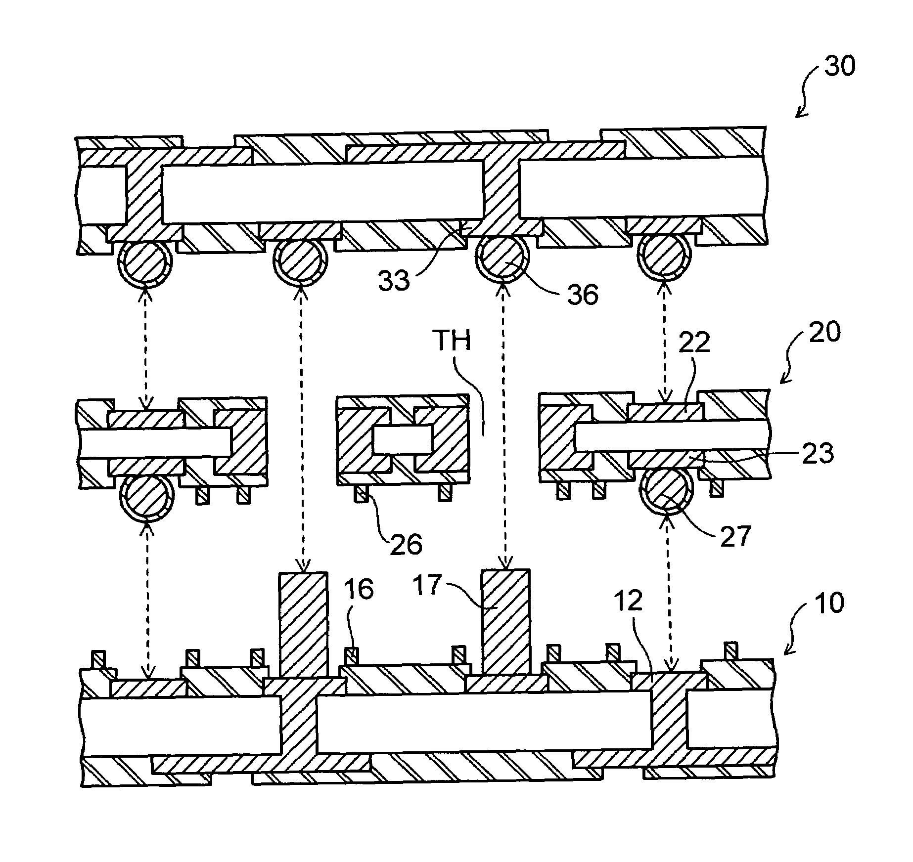
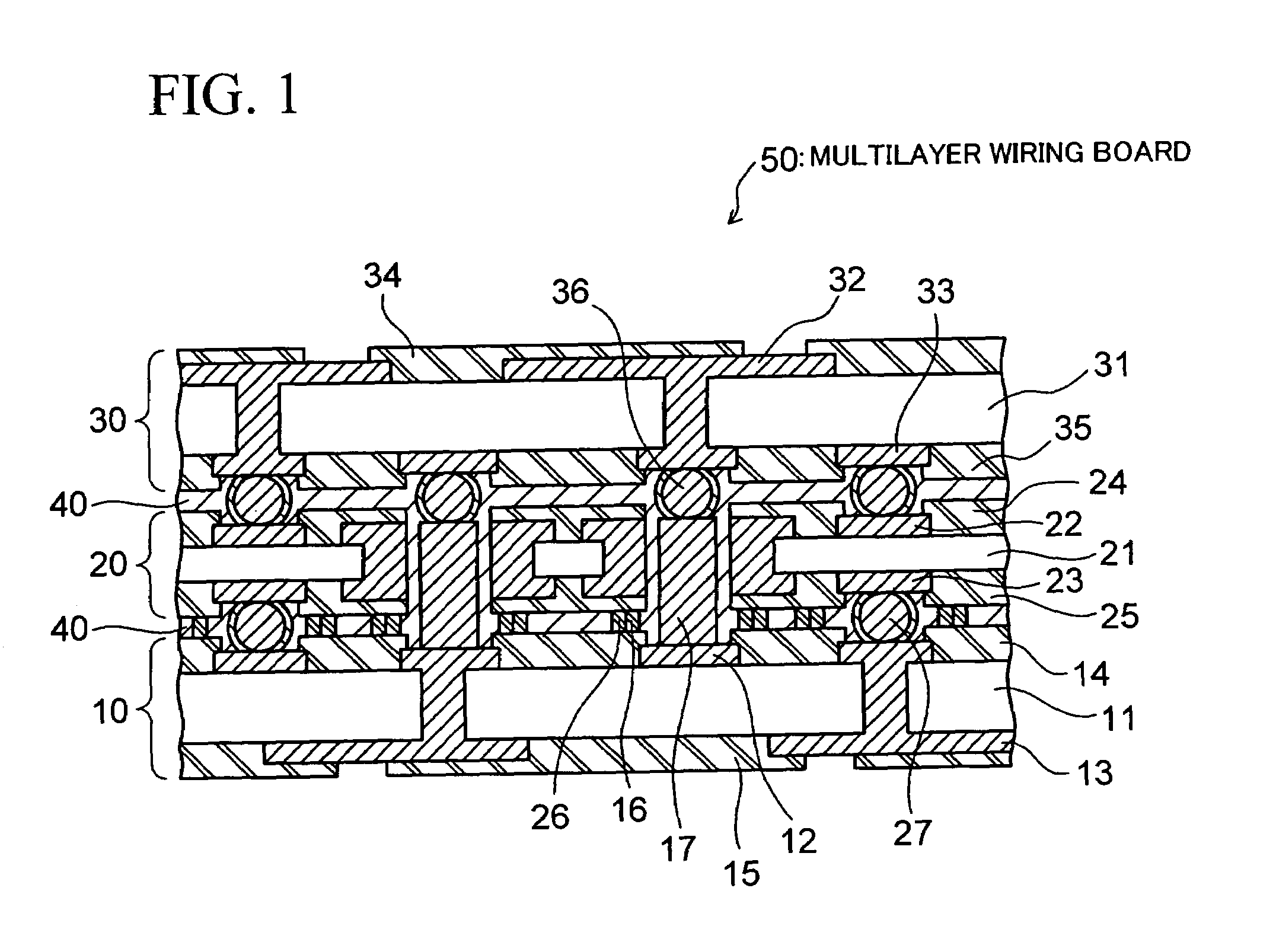
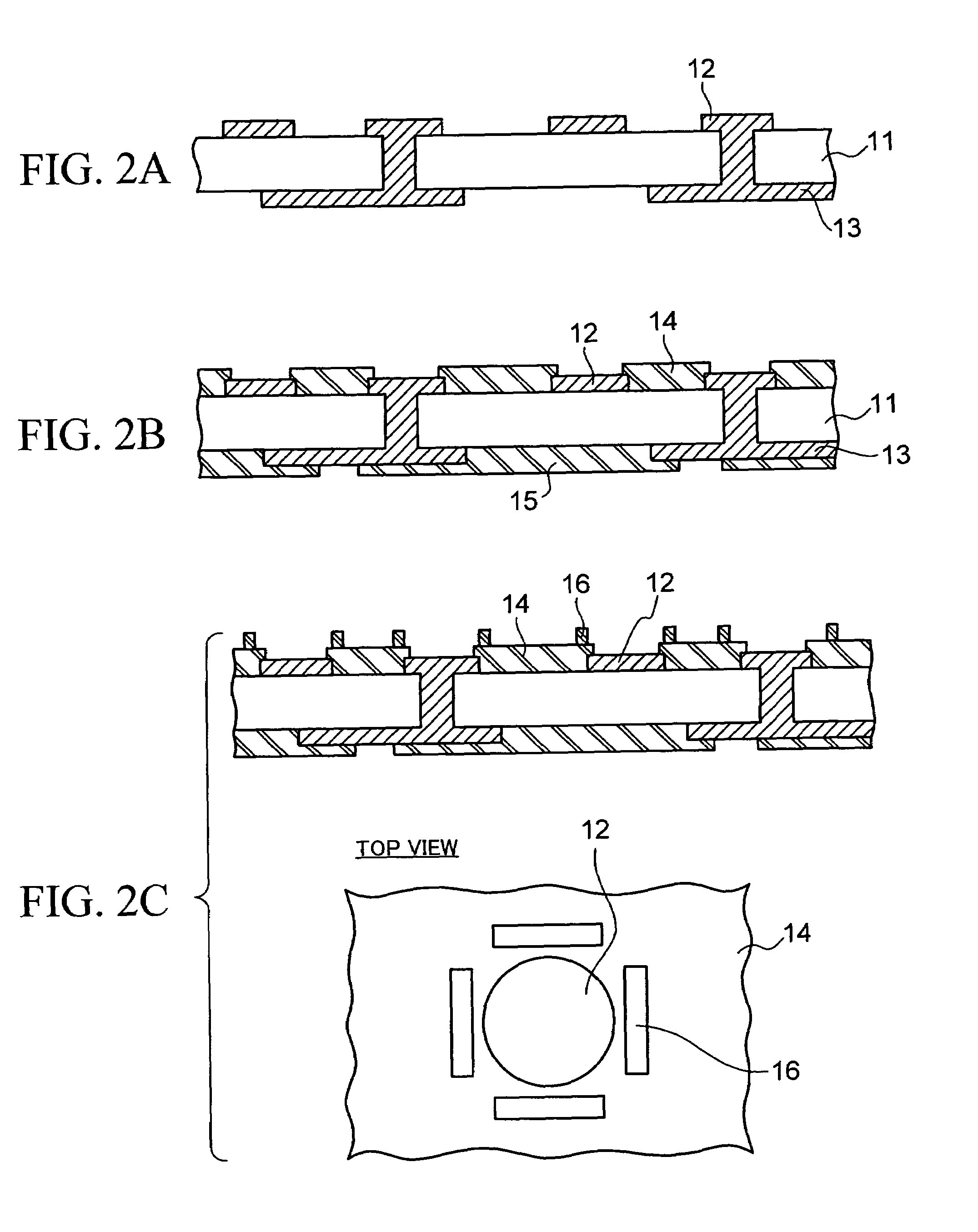
[0025]FIG. 1 shows in cross-sectional view an example of the configuration of a multilayer wiring board as manufactured using a method of manufacturing a multilayer wiring board according to an embodiment of the present invention.

[0026]As shown in FIG. 1, a multilayer wiring board 50 according to the embodiment includes three wiring boards 10, 20 and 30 stacked vertically one on top of another, and resin layers (i.e., insulating layers) 40 formed to fill in between the adjacent ones of the wiring boards 10, 20 and 30. Hereinafter, the lowermost one, namely the wiring board 10, of the wiring boards stacked will be also called a “lower wiring board” for the sake of convenience, and likewise, the intermediate one, namely the wiring board 20, will be also called a “middle wiring board,” and the uppermost one, namely the wiring board 30, will be ...


PUM

PropertyMeasurementUnit
thickaaaaaaaaaa
thickaaaaaaaaaa
thicknessaaaaaaaaaa

Abstract

First, a plurality of wiring boards are fabricated at separate steps. The first wiring board includes a Cu post formed on a wiring layer on one surface of a substrate, and a first stopper layer formed at a desired position around the Cu post. The second wiring board includes a through hole for insertion of the Cu post therethrough, a connection terminal formed on a wiring layer on one surface of a substrate, and a second stopper layer that engages the first stopper layer and functions to suppress in-plane misalignment. The third wiring board includes a connection terminal formed on a wiring layer on one surface of a substrate. Then, the wiring boards are stacked up, as aligned with one another so that the wiring layers are interconnected via the Cu post and the connection terminals, to thereby electrically connect the wiring boards. Thereafter, resin is filled into gaps between the wiring boards.

Description

CROSS-REFERENCE TO RELATED APPLICATIONS[0001]This application is based on and claims priority of Japanese Patent Application No. 2007-028521 filed on Feb. 7, 2007, the entire contents of which are incorporated herein by reference.BACKGROUND OF THE INVENTION[0002](a) Field of the Invention[0003]The present invention relates to a technique for manufacturing a wiring board for use in mounting of a chip component such as a semiconductor device, and more particularly to a method of manufacturing a multilayer wiring board (also called a “semiconductor package”) having a multilayer structure adapted to achieve high density and high performance.[0004](b) Description of the Related Art[0005]Heretofore, a build-up process has been widely used as a technique for manufacturing a multilayer wiring board. Using the build-up process makes it possible to fabricate a variety of multilayer wiring boards by means of materials (typified by resins) for an interlayer dielectric in combinations with via h...

Claims


Application Information

Patent Timeline
Patent Type & Authority Patents(United States)
IPC IPC(8): H05K3/10
CPCH05K3/462H05K3/4647H05K2201/10234H05K2203/063H05K2203/0733Y10T29/4913H05K2203/167Y10T29/49156Y10T29/49128Y10T29/49126Y10T29/49155H05K2203/1327H05K3/46
Inventor MACHIDA, YOSHIHIRO
Owner SHINKO ELECTRIC IND CO LTD
Why Eureka
Try Eureka