
Light emitting diode having active region of multi quantum well structure

a light-emitting diode and active region technology, applied in the field of light-emitting diodes, can solve the problems of decreasing decreasing luminous efficiency, and reducing luminous efficiency, so as to improve the recombination rate of electrons and holes, and reduce the qcse and/or carrier overflow

Active Publication Date: 2009-12-01
SEOUL SEMICONDUCTOR
View PDF10 Cites 1 Cited by
  • Summary
  • Abstract
  • Description
  • Claims
  • Application Information

AI Technical Summary

Benefits of technology

This configuration enhances electron-hole recombination rates, improves luminous efficiency, and allows effective light emission under varying operational conditions by reducing QCSE and carrier overflow, while lowering the driving voltage of the LED.

Problems solved by technology

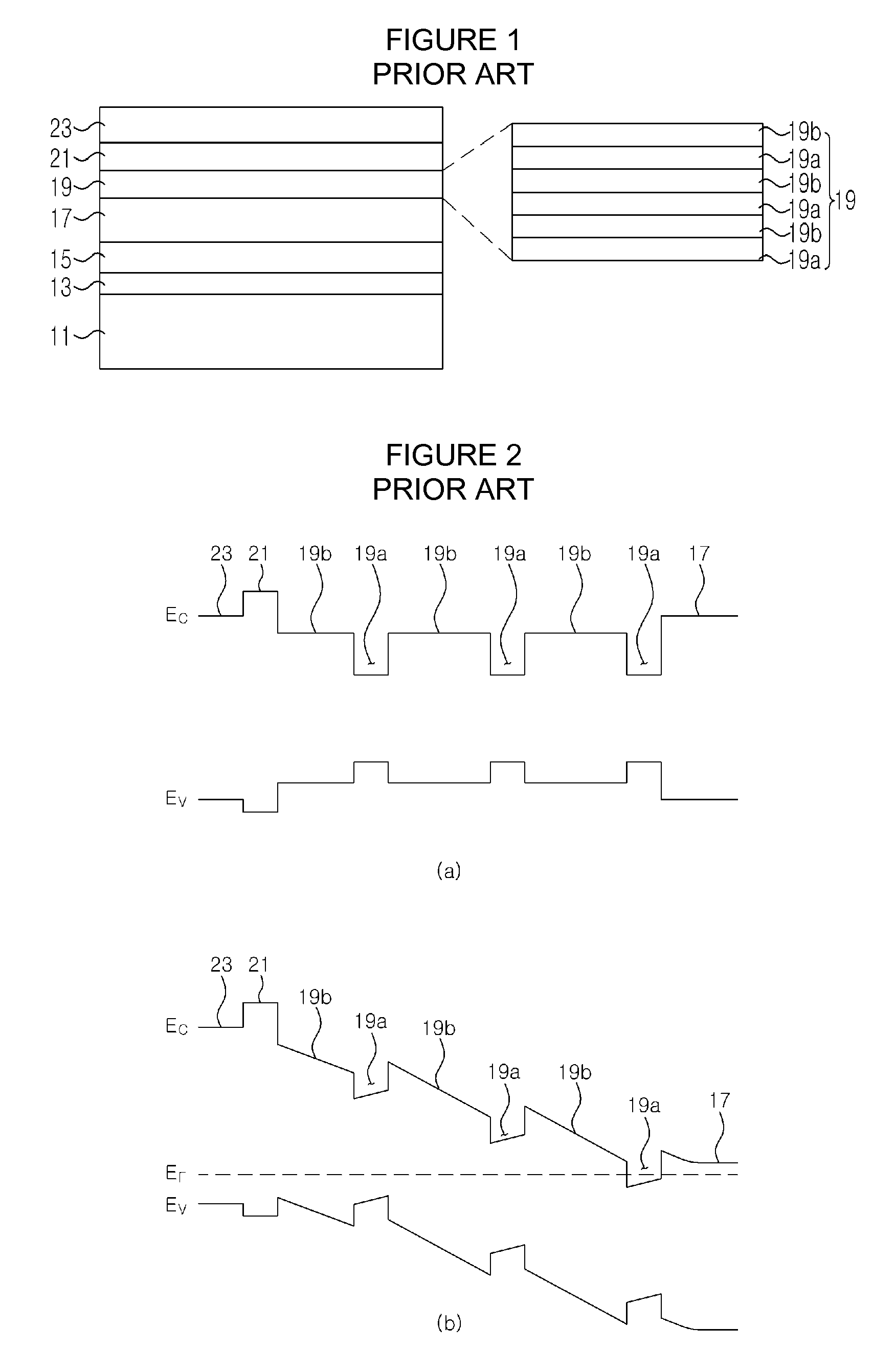
The recombination rate of electrons and holes is decreased due to the QCSE, thereby decreasing luminous efficiency.
The excessive occurrence of such carrier overflow causes the recombination rate of electrons and holes to be deteriorated, thereby decreasing luminous efficiency.
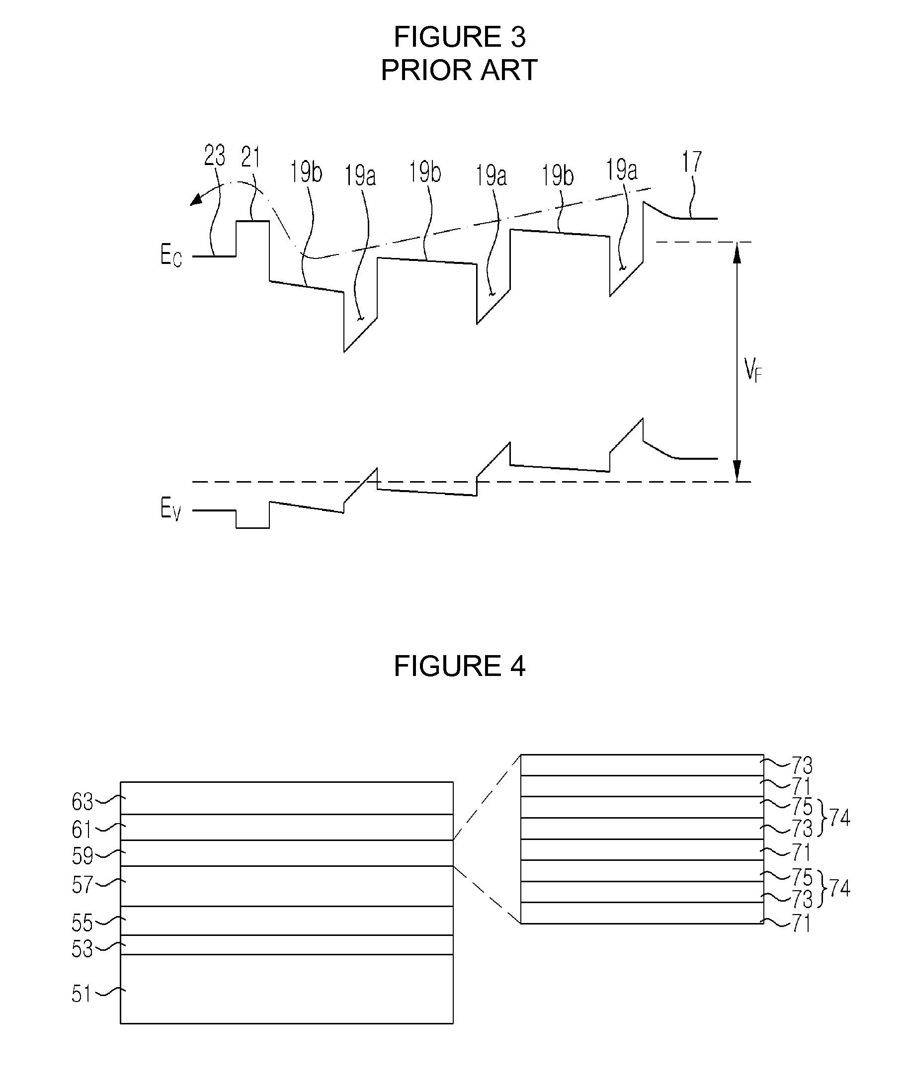
The increase of the driving voltage causes carrier overflow to be more increased, and accordingly, thereby more decreasing the luminous efficiency of the LED.
In this case, it is difficult for the conventional LED having the barrier layers 19b with the same thickness to exhibit optimum luminous characteristics under both low and high current conditions.

Method used


Image

  • Light emitting diode having active region of multi quantum well structure
  • Light emitting diode having active region of multi quantum well structure
  • Light emitting diode having active region of multi quantum well structure

Examples


Embodiment Construction

[0048]Hereinafter, preferred embodiments of the present invention will be described in detail with reference to the accompanying drawings. The following embodiments are provided only for illustrative purposes so that those skilled in the art can fully understand the spirit of the present invention. Therefore, the present invention is not limited to the following embodiments but may be implemented in other forms. In the drawings, the widths, lengths, thicknesses and the like of elements may be exaggerated for convenience of illustration. Like reference numerals indicate like elements throughout the specification and drawings.

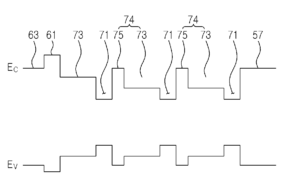
[0049]FIG. 4 is a sectional view illustrating an LED having an active region of a multi quantum well structure according to a first embodiment of the present invention, and FIG. 5 is a schematic band diagram illustrating the LED having the active region of the multi quantum well structure according to the first embodiment of the present invention. FIG. 6 is a sch...


PUM


Abstract

Disclosed is a light emitting diode having an active region of a multi quantum well structure. The active region is positioned between GaN-based N-type and P-type compound semiconductor layers. At least one of barrier layers in the active region includes an undoped InGaN layer and a Si-doped GaN layer, and the Si-doped GaN layer is in contact with a well layer positioned at a side of the P-type compound semiconductor layer therefrom. Accordingly, carrier overflow and a quantum confined stark effect can be reduced, thereby improving an electron-hole recombination rate. Further, disclosed is an active region of a multi quantum well structure including relatively thick barrier layers and relatively thin barrier layers.

Description

CROSS REFERENCE TO RELATED APPLICATIONS[0001]This application claims priority to and the benefit of Korean Patent Application No. 10-2007-0132999, filed on Dec. 18, 2007, and Korean Patent Application No. 10-2007-0133000, filed on Dec. 18, 2007, which are both incorporated by reference for all purposes as if fully set forth herein.BACKGROUND OF THE INVENTION[0002]1. Field of the Invention[0003]The present invention relates to a light emitting diode, and more particularly, to a light emitting diode having an active region of a multi quantum well structure.[0004]2. Description of the Related Art[0005]In general, since Group III element nitrides, such as GaN, AlN and InGaN, have excellent thermal stability and a direct transition type energy band structure, they have recently come into the spotlight as materials for light emitting diodes (LEDs) in blue and ultraviolet regions. Particularly, an InGaN compound semiconductor has been considerably noticed due to its narrow band gap. LEDs u...

Claims


Application Information

Patent Timeline
Patent Type & Authority Patents(United States)
IPC IPC(8): H01L33/00H01L33/06H01L33/32
CPCH01L33/32H01L33/06
Inventor LEE, DONG SEONHWANG, EU JIN
Owner SEOUL SEMICONDUCTOR
Learn More