Machining method to controllably produce chips with determinable shapes and sizes

a technology of machining body and chip, which is applied in the direction of magnetic bodies, program control, instruments, etc., can solve the problems of inability to induce large strains in very strong materials, such as tool steels, and considerable uncertainty of deformation field, so as to achieve accurate and repeatable results, large strain deformation, and high strain rate

Inactive Publication Date: 2009-12-08
PURDUE RES FOUND INC
View PDF40 Cites 27 Cited by
  • Summary
  • Abstract
  • Description
  • Claims
  • Application Information

AI Technical Summary

Benefits of technology

[0011]The above aspects of the invention are based on the determination that nanocrystalline structures can be formed in materials by machining under appropriate conditions to produce very large strain deformation, including high strain rates, such as a plastic strain of about 0.5 to about 10 and a strain rate of up to 106 per second. Machining processes believed to be capable of producing suitable nanocrystalline structures include cutting and abrasion techniques. Cutting speed does not appear to be determinative, such that essentially any cutting speed can be used if a cutting tool is used to perform the machining operation. Because the production method for the chips is a machining operation whose parameters can be precisely controlled, the desired nanocrystalline microstructure for the chips can be accurately and repeatably obtained for a given body material. Furthermore, the modulation-assisted machining step of this invention enables the controlled production of chips of various grain sizes and macroscopic shapes for use in a variety of application. The production of nanocrystalline chips can be achieved with this invention with minimal impact on the article being machined, such that nanocrystalline chips can be produced as a useful byproduct of an existing manufacturing operation.
[0012]In view of the above, the present invention provides a controllable and low-cost method for synthesizing nanocrystalline solids that can be used to produce monolithic and composite products. The method of this invention also makes possible the capability of producing nanocrystalline solids from materials that have been difficult or impossible to process using prior art techniques, such as very hard materials that cannot be processed by multistage deformation processes, and alloys that cannot be processed by the condensation method.

Problems solved by technology

However, there are significant limitations and disadvantages with this processing technique.
A significant limitation is the inability to induce large strains in very strong materials, such as tool steels.
Other limitations include the inability to impose a strain of much greater than one in a single stage of deformation, the considerable uncertainty of the deformation field, and the minimal control over the important variables of the deformation field—such as strain, temperature, strain rate and phase transformations—that are expected to have a major influence on the evolution of microstructure and material properties.
While suitable for making powders and small compacted samples with excellent control over particle size, the condensation method is at present not practical for most applications other than experimental.
A particularly limiting aspect of the condensation method is the inability to form nanocrystalline materials of alloys because of the difficulty of controlling the composition of the material from the vapor phase.
Another limiting aspect of the condensation method is that high green densities are much harder to achieve as a result of the nano-size particles produced.
However, these techniques cannot produce nanocrystalline materials at a cost acceptable for practical applications.

Method used


Image

  • Machining method to controllably produce chips with determinable shapes and sizes
  • Machining method to controllably produce chips with determinable shapes and sizes
  • Machining method to controllably produce chips with determinable shapes and sizes

Examples


Embodiment Construction

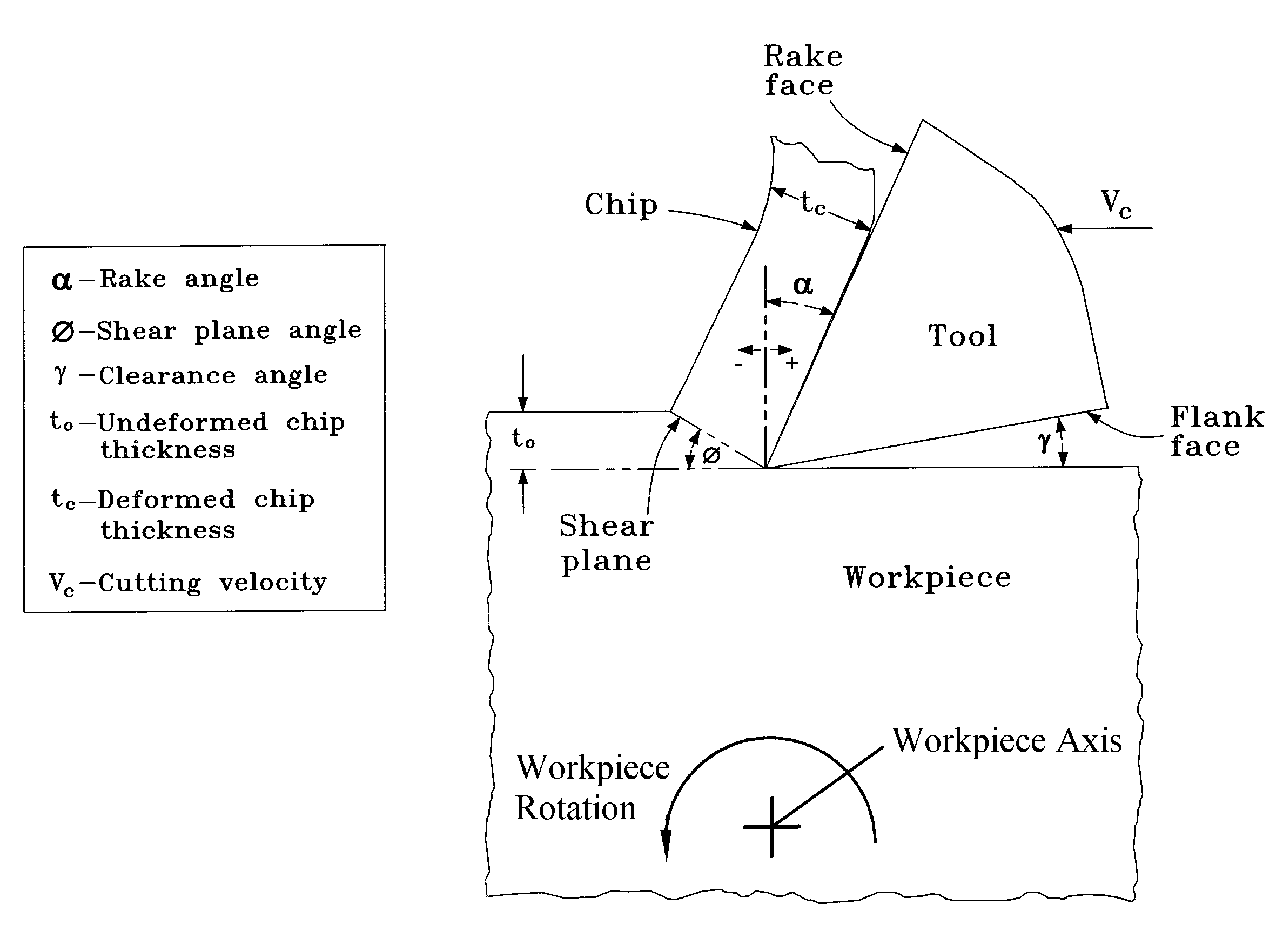
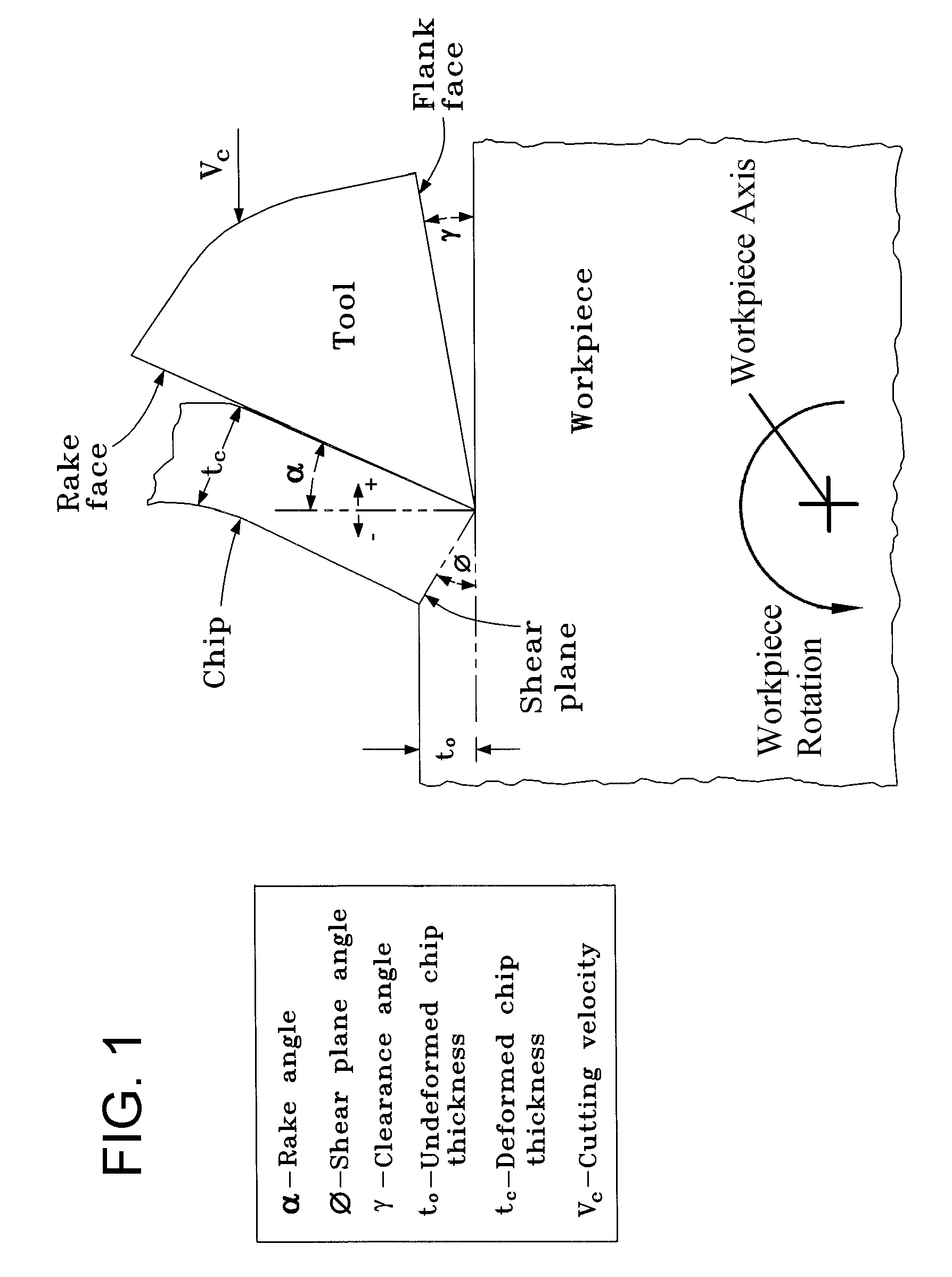
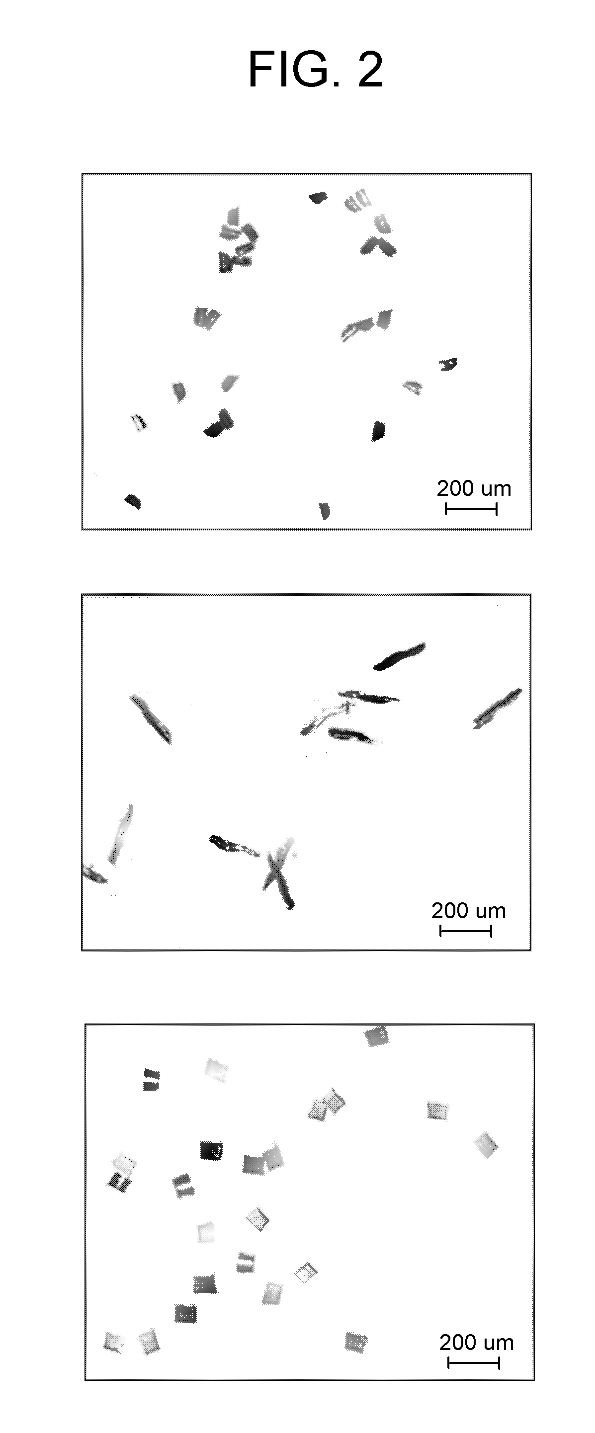
[0016]The invention provides a method for the direct production of chips by modulated machining. Chips are directly manufactured from bulk materials, including metals, metal alloys, intermetallics, and ceramics. Furthermore, machining conditions can be chosen to induce severe plastic deformation that results the creation of chips with nanocrystalline microstructures from bulk materials that may have microstructures that are essentially free of nanocrystals. Modulation conditions are superimposed on the machining operation to control the size and shape of the chips, providing the capability of chips ranging from a few nanometers to several millimeters in length. Because chips of controllable morphology, size, and shape can be produced directly by the modulated machining process of this invention, the need for additional secondary comminution steps is eliminated. With controlled modulation, it is possible to produce chips with sizes and shape that include equiaxed particulates, ribbon...


PUM

PropertyMeasurementUnit
lengthaaaaaaaaaa
lengthaaaaaaaaaa
lengthaaaaaaaaaa

Abstract

A method of controllably producing chips with a desired shape and size. The method generally entails machining a body with a cutting tool while superimposing modulation on the cutting tool so as to move the cutting tool relative to the body being machined and cause instantaneous and periodic separation between the cutting tool and the body at a point of contact between the cutting tool and the body, wherein each separation between the cutting tool and the body yields a chip. In this manner, the shapes and sizes of the chips are determined at least in part by the modulation cycle, and particularly the length of time the cutting tool is engaged with the body being machined.

Description

CROSS REFERENCE TO RELATED APPLICATIONS[0001]This patent application claims the benefit of U.S. Provisional Application No. 60 / 677,248, filed May 3, 2005, and is related to U.S. Pat. No. 7,294,165, which is a division application Ser. No. 10 / 051,626 filed on Oct. 27, 2001, now of U.S. Pat. No. 6,706,324, which claimed the benefit of U.S. Provisional Application No. 60 / 244,087, filed Oct. 28, 2000. The contents of these prior applications and patents are incorporated herein by reference.BACKGROUND OF THE INVENTION[0002]The present invention generally relates to methods of machining a body to produce chips, and more particularly to a machining method in which a superimposed modulation is imposed on a cutting tool to produce chips by causing instantaneous and periodic separation between the cutting tool and the body.[0003]Significant benefits can be gained by deforming metal alloys through the application of very large plastic strains. Principal among these are microstructure refinemen...

Claims


Application Information

Patent Timeline
Patent Type & Authority Patents(United States)
IPC IPC(8): C21D7/04
CPCB22F9/04B23B1/00B23B29/125Y10T408/23B22F2998/00B22F2999/00G05B2219/37598B22F2009/046Y10T408/03Y10T409/303808Y10T82/10Y10S82/904B22F1/0044B22F1/0055B22F1/004B22F2202/01B22F1/07B22F1/062B22F1/068
Inventor MANN, JAMES B.SHANKAR, M. RAVICHANDRASEKAR, SRINIVASANCOMPTON, W. DALEMOSCOSO, WILFREDO
Owner PURDUE RES FOUND INC
Why Eureka
Try Eureka