Method of forming nano-crystalline structures and product formed thereof

a nano-crystalline structure and nano-crystalline technology, applied in the direction of crystal growth process, blast furnace, metal-working apparatus, etc., can solve the problems of inability to induce large strains of very strong materials, such as tool steels, and significant uncertainties in the deformation field

Inactive Publication Date: 2007-11-13
PURDUE RES FOUND INC
View PDF9 Cites 4 Cited by
  • Summary
  • Abstract
  • Description
  • Claims
  • Application Information

AI Technical Summary

Benefits of technology

[0011]The above features of the invention are based on the determination that nanocrystalline structures can be formed in materials by machining under appropriate conditions to produce very large strain deformation, including high strain rates, such as a plastic strain of about 0.5 to about 10 and a strain rate of up to 106 per second. Machining processes believed to be capable of producing suitable nanocrystalline structures include cutting and abrasion techniques. Cutting speed does not appear to be determinative, such that essentially any cutting speed can be used if a cutting tool is used to perform the machining operation. Because the production method for the chips is a machining operation whose parameters can be precisely controlled, the desired nanocrystalline microstructure for the chips can be accurately and repeatably obtained for a given body material. Furthermore, the machining operation can be adjusted to produce chips of various grain sizes and macroscopic shapes for use in a variety of application. The production of nanocrystalline chips can often be achieved with this invention without having any negative impact on the article being machined, such that nanocrystalline chips can be produced as a useful byproduct of an existing manufacturing operation.
[0012]In view of the above, the present invention provides a controllable and low-cost method for synthesizing nanocrystalline solids that can be used to produce monolithic and composite products. The method of this invention also makes possible the capability of producing nanocrystalline solids from materials that have been difficult or impossible to process using prior art techniques, such as very hard materials that cannot be processed by multi-stage deformation processes, and alloys that cannot be processed by the condensation method.

Problems solved by technology

However, there are significant limitations and disadvantages with this processing technique.
A significant limitation is the inability to induce large strains in very strong materials, such as tool steels.
Other limitations include the inability to impose a strain of much greater than one in a single stage of deformation, the considerable uncertainty of the deformation field, and the minimal control over the important variables of the deformation field—such as strain, temperature, strain rate and phase transformations—that are expected to have a major influence on the evolution of microstructure and material properties.
While suitable for making powders and small compacted samples with excellent control over particle size, the condensation method is at present not practical for most applications other than experimental.
A particularly limiting aspect of the condensation method is the inability to form nanocrystalline materials of alloys because of the difficulty of controlling the composition of the material from the vapor phase.
Another limiting aspect of the condensation method is that high green densities are much harder to achieve as a result of the nano-size particles produced.
However, these techniques cannot produce nanocrystalline materials at a cost acceptable for practical applications.

Method used


Image

  • Method of forming nano-crystalline structures and product formed thereof
  • Method of forming nano-crystalline structures and product formed thereof
  • Method of forming nano-crystalline structures and product formed thereof

Examples


Embodiment Construction

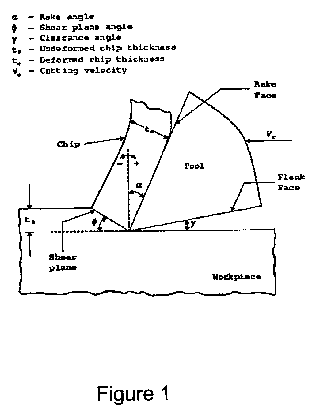
[0020]An investigation leading to this invention was undertaken to determine the microstructure and mechanical properties of chips produced by machining steels, and to explore the conditions under which they are produced. Steel cylinders of AISI 52100, 4340 and M2 tool steel having diameters of about 15.7 mm were heat-treated by through-hardening and tempering to hardness values of about 60 to 62 Rc, about 56 to 57 Rc, and about 60 to 62 Rc, respectively. The initial microstructures of the steels prior to machining were tempered martensite. The compositions (in weight percent), austenitization temperatures (AC3) and approximate grain size (GS) of the steel specimens are summarized in Table 1 below.

[0021]

TABLE 1Steel Type (AISI)434052100M2C0.38-0.431.000.8Mn 0.6-0.80.310.35Si0.15-0.30.260.35Cr 0.7-0.91.454.52Ni1.65-2.000.140.2Mo 0.2-0.30.045.39P0.035 max0.009 max0.027 maxS0.040 max0.019 max0.005 maxV——2.09Cu—0.090.13Al——0.02Co——0.39W——6.86FebalancebalancebalanceAC3 (° C.) 815-845775-...


PUM

PropertyMeasurementUnit
sizeaaaaaaaaaa
sizeaaaaaaaaaa
sizesaaaaaaaaaa

Abstract

A product in which at least a portion of the product has a nanocrystalline microstructure, and a method of forming the product. The method generally entails machining a body in a manner that produces chips consisting entirely of nano-crystals as a result of the machining operation imposing a sufficiently large strain deformation. The body can be formed of a variety of materials, including metal, metal alloy and ceramic materials. Furthermore, the body may have a microstructure that is essentially free of nano-crystals, and may even have a single-crystal microstructure. The chips produced by the machining operation may be in the form of particulates, ribbons, wires, filaments and / or platelets. The chips are then used to form the product. According to one aspect of the invention, the chips are consolidated to form the product, such that the product is a monolithic material that may contain nano-crystals. According to another aspect of the invention, the chips are dispersed in a matrix material, such that the product is a composite material in which the chips serve as a reinforcement material.

Description

CROSS REFERENCE TO RELATED APPLICATIONS[0001]This application is a divisional patent application of U.S. patent application Ser. No. 10 / 051,626, filed Oct. 27, 2001 now U.S. Pat. No. 6,706,324, and claims the benefit of U.S. Provisional Application No. 60 / 244,087, filed Oct. 28, 2000.FEDERAL RESEARCH STATEMENT[0002]Not ApplicableBACKGROUND OF INVENTION[0003]1. Field of the Invention[0004]The present invention generally relates to methods of producing materials with nanocrystalline microstructures, and more particularly to producing such materials by machining and then using the nanocrystalline material to form a product.[0005]2. Description of the Related Art[0006]Significant benefits can be gained by deforming metal alloys through the application of very large plastic strains. Principal among these are microstructure refinement and enhanced mechanical and physical properties. Of particular current interest is the use of “severe” plastic deformation (SPD) to produce bulk solids with...

Claims


Application Information

Patent Timeline
Patent Type & Authority Patents(United States)
IPC IPC(8): B22F8/00B22F1/054B22F9/00B22F9/04C04B20/02C04B35/622C22C1/04C22C49/14C30B33/00
CPCB22F1/0018B22F9/005B22F9/04B82Y30/00C04B20/026C04B35/622C22C49/14C30B33/00B22F1/0044C04B20/008C30B29/605C22C1/1036B22F1/0003B22F3/10B22F3/20B22F3/26B22F1/0025B22F2001/0033B22F2998/00B22F2999/00C04B2235/5454C04B2235/78C04B2235/781C04B2235/785Y10S241/14Y10S75/954B22F2009/046B22F1/0551B22F1/07B22F1/054B22F1/056B22F1/0547B22F1/09B22F1/12
Inventor CHANDRASEKAR, SRINIVASANCOMPTON, WALTER D.FARRIS, THOMAS N.TRUMBLE, KEVIN P.
Owner PURDUE RES FOUND INC
Why Eureka
Try Eureka