Electrophotographic printing of electronic devices

a technology of electronic devices and electrotrophotography, applied in the field of electrotrophotographic printing of electronic devices, can solve the problems of high capital cost, limited ability to adjust process parameters and implement design changes, and high capital cost of device fabrication plants, and achieve the effect of reducing manufacturing costs and being convenient to apply

Active Publication Date: 2009-12-29
HEWLETT PACKARD DEV CO LP
View PDF16 Cites 17 Cited by
  • Summary
  • Abstract
  • Description
  • Claims
  • Application Information

AI Technical Summary

Benefits of technology

[0004]It has been recognized that it would be advantageous to develop improved methods and systems for forming electrical devices which entails reduced manufacturing costs and is conveniently applied to a wide variety of substrates. In accordance with one aspect of the present invention, a method of forming an electrical device can include electrophotographically printing a particulate material on a device substrate. The particulate material forms at least a portion of the electrical device. More specifically, suitable particulate materials can have an aspect ratio of at least about 2:1.

Problems solved by technology

Frequently these methods involve considerable capital costs and restrictions on production times. Most device fabrication plants experience a constant struggle with high capital costs and limited ability to adjust process parameters and implement design changes.
Yet many of these methods are often unreliable or otherwise undesirable for commercial scale production.
Each of the above methods has disadvantages which limit their effectiveness, such as expense, reliability, and complexity.

Method used


Image

  • Electrophotographic printing of electronic devices
  • Electrophotographic printing of electronic devices

Examples


Embodiment Construction

)

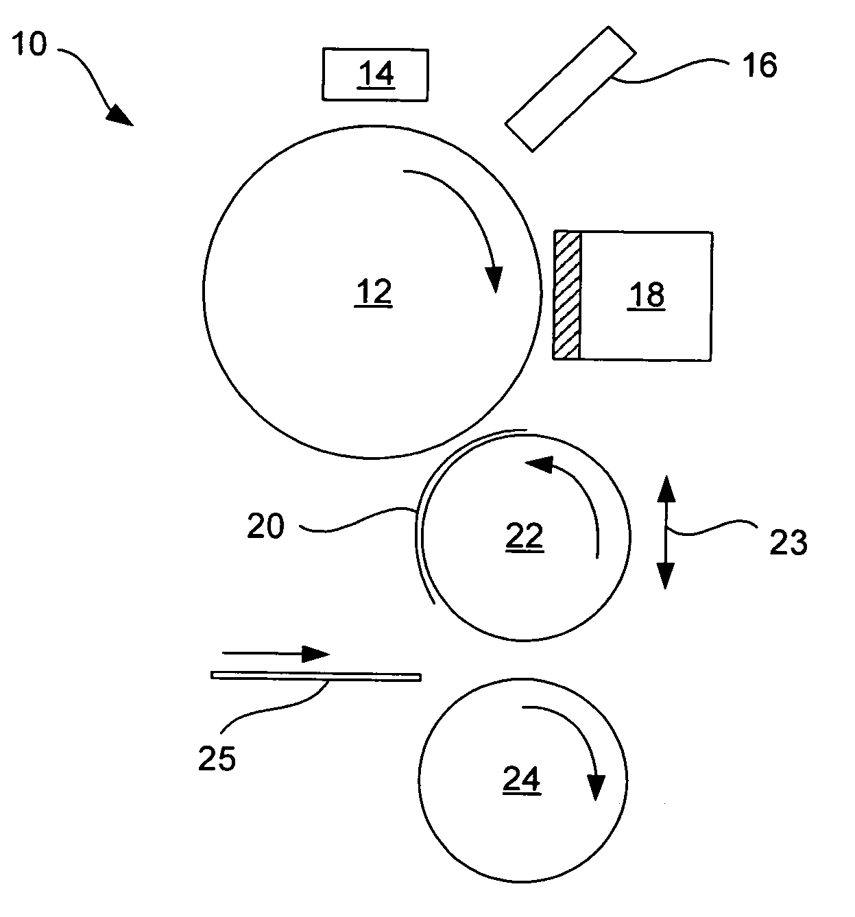
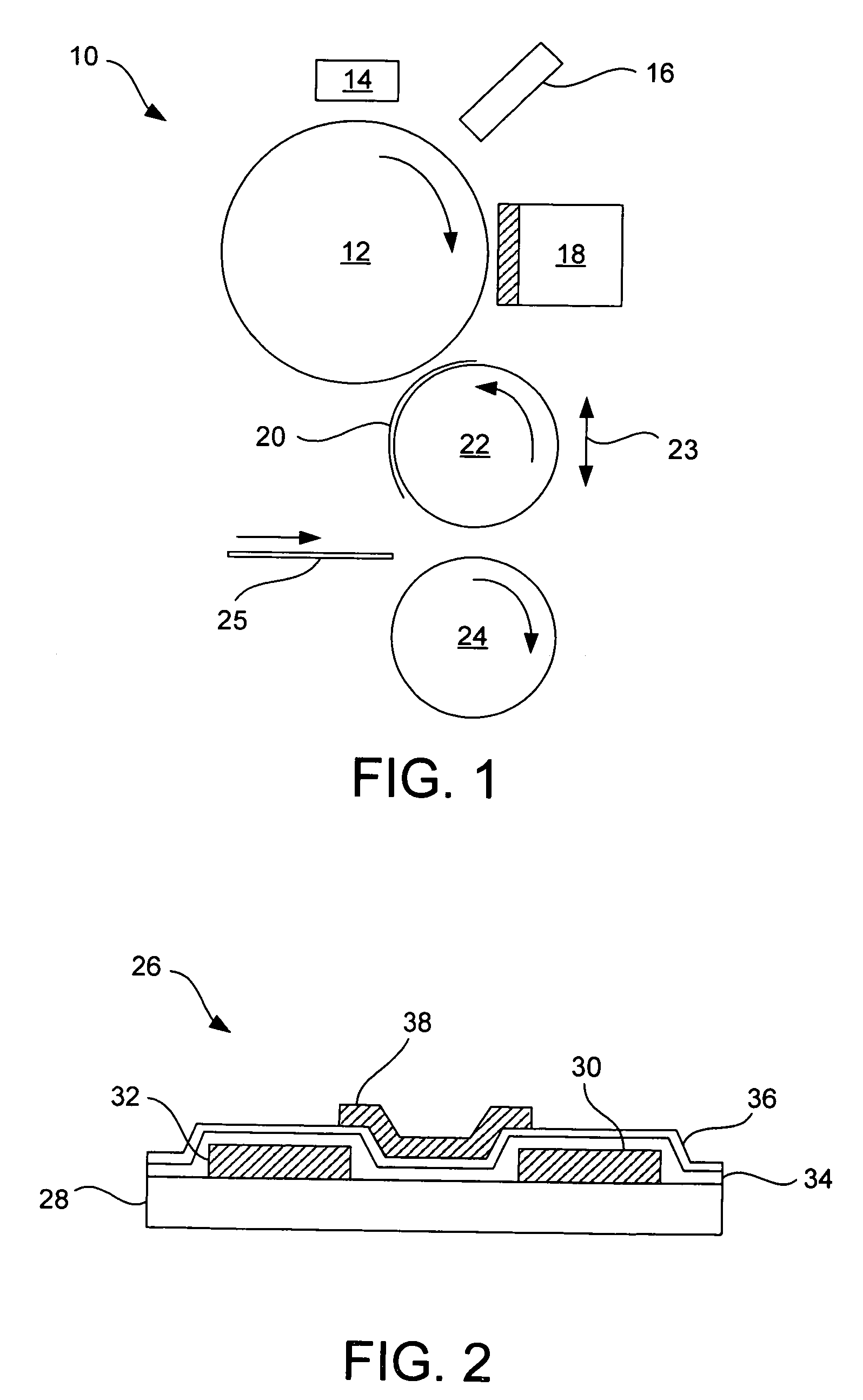
[0010]Reference will now be made to exemplary embodiments and specific language will be used herein to describe the same. It will nevertheless be understood that no limitation of the scope of the invention is thereby intended. Alterations and further modifications of the inventive features described herein, and additional applications of the principles of the invention as described herein, which would occur to one skilled in the relevant art and having possession of this disclosure, are to be considered within the scope of the invention. Further, before particular embodiments of the present invention are disclosed and described, it is to be understood that this invention is not limited to the particular process and materials disclosed herein as such may vary to some degree. It is also to be understood that the terminology used herein is used for the purpose of describing particular embodiments only and is not intended to be limiting, as the scope of the present invention will be de...


PUM


Abstract

A method of forming electrical devices can include electrophotographically printing a particulate material on a device substrate, and the particulate material can form at least a portion of the electrical device. An optional intermediate transfer member can also be used to improve reliability and performance of the process. Dry or liquid electrophotographic methods can be effectively used to form electronic devices on a wide variety of substrates not conventionally available in device fabrication.

Description

FIELD OF THE INVENTION[0001]The present invention relates generally to formation of electronic devices. More particularly, the present invention relates to processes and systems which use electrophotography to form electronic devices.BACKGROUND OF THE INVENTION[0002]Production of circuits and conductive traces has been accomplished in many different ways, each process having a range of benefits and drawbacks. Further, various methods for manufacturing printed circuit boards and electronic components are known. Typical methods for manufacturing printed circuits include print and etch, screen printing, and photoresist methods, e.g., applying photoresist, exposing, and developing. Frequently these methods involve considerable capital costs and restrictions on production times. Most device fabrication plants experience a constant struggle with high capital costs and limited ability to adjust process parameters and implement design changes. A number of methods have been explored to decre...

Claims


Application Information

Patent Timeline
Patent Type & Authority Patents(United States)
IPC IPC(8): G03G5/00
CPCG03G15/221H01L21/283H01L21/288H01L21/76838H01L29/66757G03G15/6591H05K3/1266G03G2215/00523H05K1/16H05K2201/0257H05K2203/0143H05K2203/0517H01L29/7869
Inventor STASIAK, JAMES WILLIAMMCCLELLAND, PAUL
Owner HEWLETT PACKARD DEV CO LP
Why Eureka
Try Eureka