Manufacturing method for partially-good memory modules with defect table in EEPROM

a technology of memory modules and defect tables, applied in the field of memory module manufacturing, can solve the problems of noisy test environment, wafer-sort test may not catch all defects, and manufacturing defects to be somewhat common

a technology of memory modules and defect tables, applied in the field of memory module manufacturing, can solve the problems of noisy test environment, wafer-sort test may not catch all defects, and manufacturing defects to be somewhat common

US7642105B2Active Publication Date: 2010-01-05KINGSTON DIGITAL CO LTD

Image

  • Manufacturing method for partially-good memory modules with defect table in EEPROM
  • Manufacturing method for partially-good memory modules with defect table in EEPROM
  • Manufacturing method for partially-good memory modules with defect table in EEPROM

Examples


Embodiment Construction

[0037]The present invention relates to an improvement in memory module manufacturing. The following description is presented to enable one of ordinary skill in the art to make and use the invention as provided in the context of a particular application and its requirements. Various modifications to the preferred embodiment will be apparent to those with skill in the art, and the general principles defined herein may be applied to other embodiments. Therefore, the present invention is not intended to be limited to the particular embodiments shown and described, but is to be accorded the widest scope consistent with the principles and novel features herein disclosed.

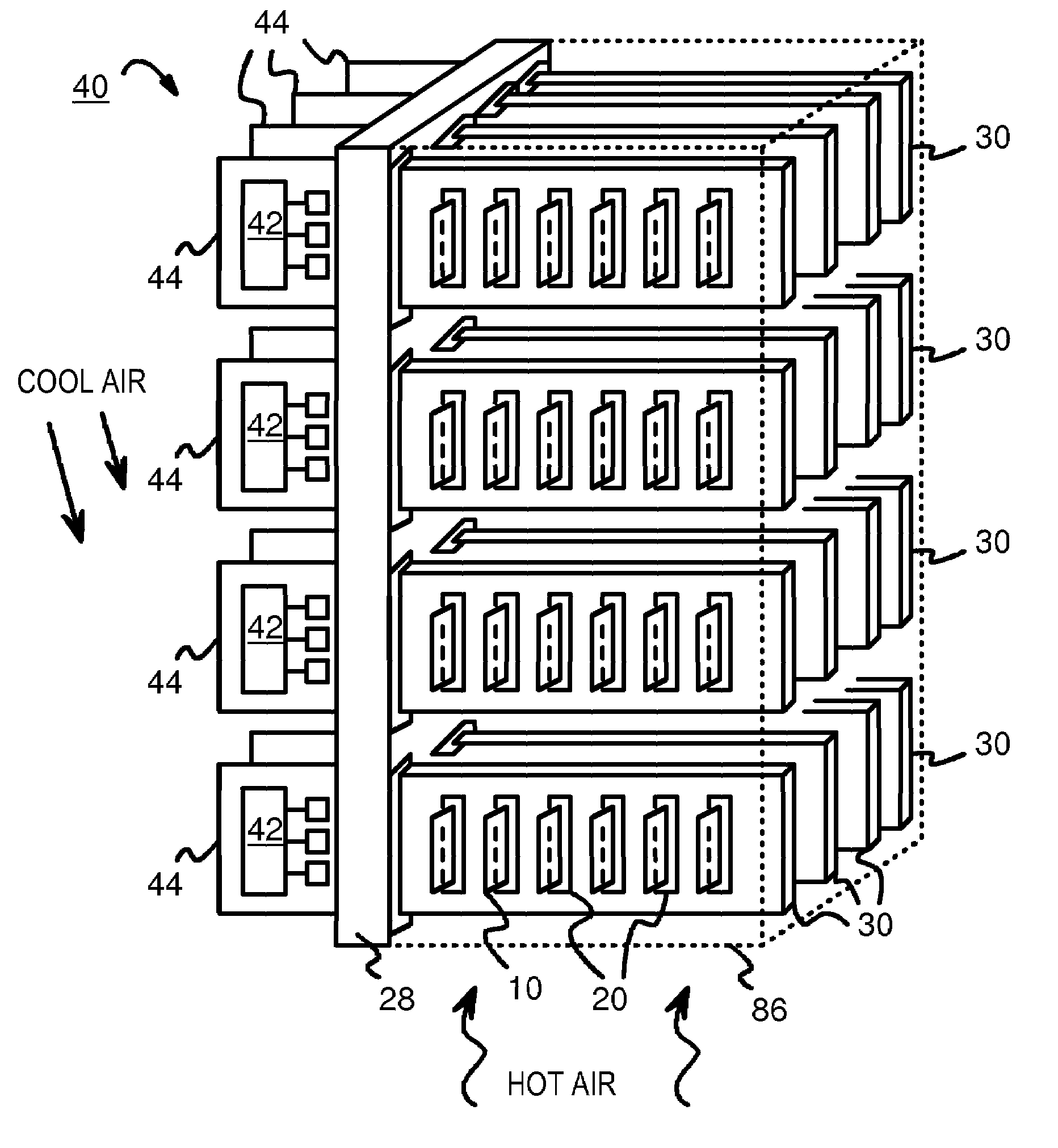
[0038]FIG. 4 highlights a test flow that burns in assembled memory modules rather than individual partially-good DRAM chips. Wafers of good and partially-good DRAM die are packaged into packages such as ball-grid-array (BGA) or thin-small-outline packages (TSOP) and delivered to the memory module manufacturer. The packaged...


PUM


Abstract

A manufacturing method makes memory modules from partially-good DRAM chips soldered to its substrate. The partially-good DRAM chips have a number of defective memory cells that is below a test threshold, such as 10%. Packaged DRAM chips are optionally pre-screened and considered to pass when the number of defects found is less than the test threshold. A defect table is created during testing and written to a serial-presence-detect electrically-erasable read-only memory (SPD-EEPROM) on the memory module. The memory module is finally tested on a target-system tester that reads the defect table during booting, and redirects memory access to defective memory locations identified by the defect table. The memory modules may be burned in or tested at various temperatures and voltages to increase reliability.

Description

RELATED APPLICATIONS[0001]This application may be related to U.S. Ser. Nos. 11 / 308,869, 11 / 309,297, 11 / 309,298, and U.S. Pat. No. 7,277,337, having a common assignee and at least one inventor in common, but presenting patentably distinct claims.FIELD OF THE INVENTION[0002]This invention relates to memory-module manufacturing, and more particularly to making memory modules using partially-good memory chips.BACKGROUND OF THE INVENTION[0003]Memory modules are widely used in a variety of electronic systems, especially Personal Computers (PC's). Memory modules are built to meet specifications set by industry standards, thus ensuring a wide potential market. High-volume production and competition have driven module costs down dramatically, benefiting buyers of a wide variety of electronic systems.[0004]Memory modules are made in many different sizes and capacities, such as older 30-pin and 72-pin single-inline memory modules (SIMMs) and newer 168-pin, 184-pin, and 240-pin dual inline memo...

Claims


Application Information

Patent Timeline
05 Jan 2010
Publication
US7642105B2
IPC
H01L21/66; G01R31/26; G11C29/00
CPC
G11C29/06; G11C29/44; G11C29/56; G11C29/56016; G11C29/88; G11C29/886; H01L22/20; G11C5/04
Inventors
CO, RAMON S.; CHEN, MIKE