Packaging for high power integrated circuits

a high-power integrated circuit and packaging technology, applied in the direction of semiconductor devices, semiconductor/solid-state device details, electrical apparatus, etc., to achieve the effect of increasing junction temperature, reducing the number of thermal interfaces needed, and increasing the thermal resistance of the conduction path

Active Publication Date: 2010-01-05
MAYO FOUND FOR MEDICAL EDUCATION & RES
View PDF16 Cites 10 Cited by
  • Summary
  • Abstract
  • Description
  • Claims
  • Application Information

AI Technical Summary

Benefits of technology

[0006]An advantage of this invention is that it allows for direct device-side cooling of the device. The device is mounted to a substrate and an enclosed space is formed around the device which contains the working supercritical fluid. The much larger enclosure is cooled by more conventional means. The result is that cooling can take place through both sides of the device, rather than just the backside. This technique can be utilized with devices that are flip-chip attached or wirebonded to the substrate. Passivation of the device is not required with selection of the proper working fluid. Direct cooling is done in phase change cooling techniques such as thermosyphons and microchannel flows. The use of a supercritical fluid eliminates the problems of vapor entrapment and thermal shock due to the incipience temperature drop that are seen with phase change cooling.
[0008]This invention also offers some mechanical advantages over other thermal management methods. The number of thermal interfaces needed is reduced because the working fluid is in direct contact with the heat generating device. One of the issues with attachment of heat spreaders and heat sinks is the need to compensate for the coefficient of thermal expansion (CTE) mismatch between the chip, heat spreader, and the heat sink. Commonly, thermally conductive adhesive must be used to transition between the heat spreader, which typically has a coefficient of thermal expansion (“CTE”) matched to the power device, and the heat sink, which is typically a high CTE material. This interface increases the thermal resistance of the conduction path which in turn increases the junction temperature. The invention offers advantages for high shock and vibration environments, because the thermal path presented by the supercritical working fluid is not structural.
[0009]This invention may easily be used in combination with other thermal management techniques. For wirebonded chips, for example, heat spreaders and heat sinks can be attached to the back of the chip or package while the heat is also removed from the top by the supercritical fluid. Chip level cooling techniques such as thermal vias, thinned chips, on-chip integration of Peltier devices, microchannels in the back of the chip may also be used in conjunction with the supercritical fluid.

Problems solved by technology

One of the issues with attachment of heat spreaders and heat sinks is the need to compensate for the coefficient of thermal expansion (CTE) mismatch between the chip, heat spreader, and the heat sink.

Method used


Image

  • Packaging for high power integrated circuits
  • Packaging for high power integrated circuits
  • Packaging for high power integrated circuits

Examples


Embodiment Construction

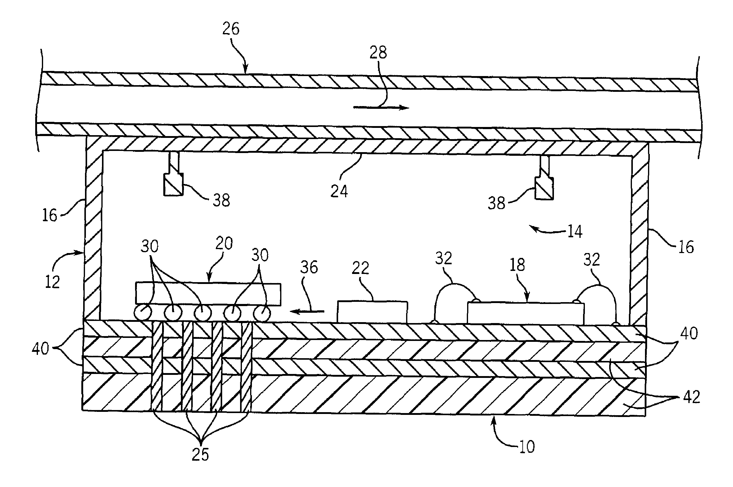
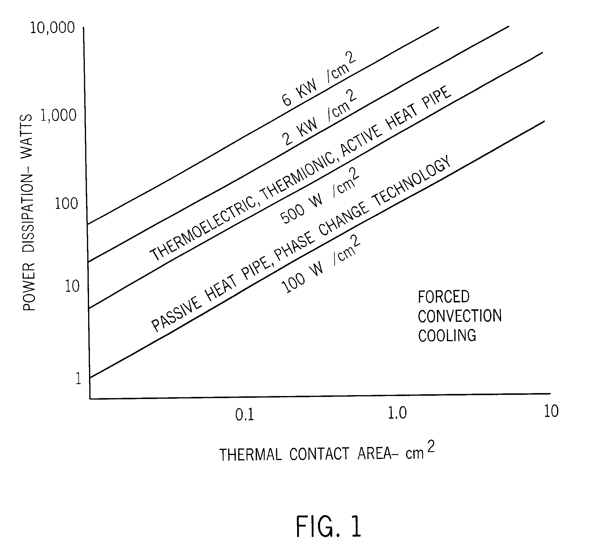
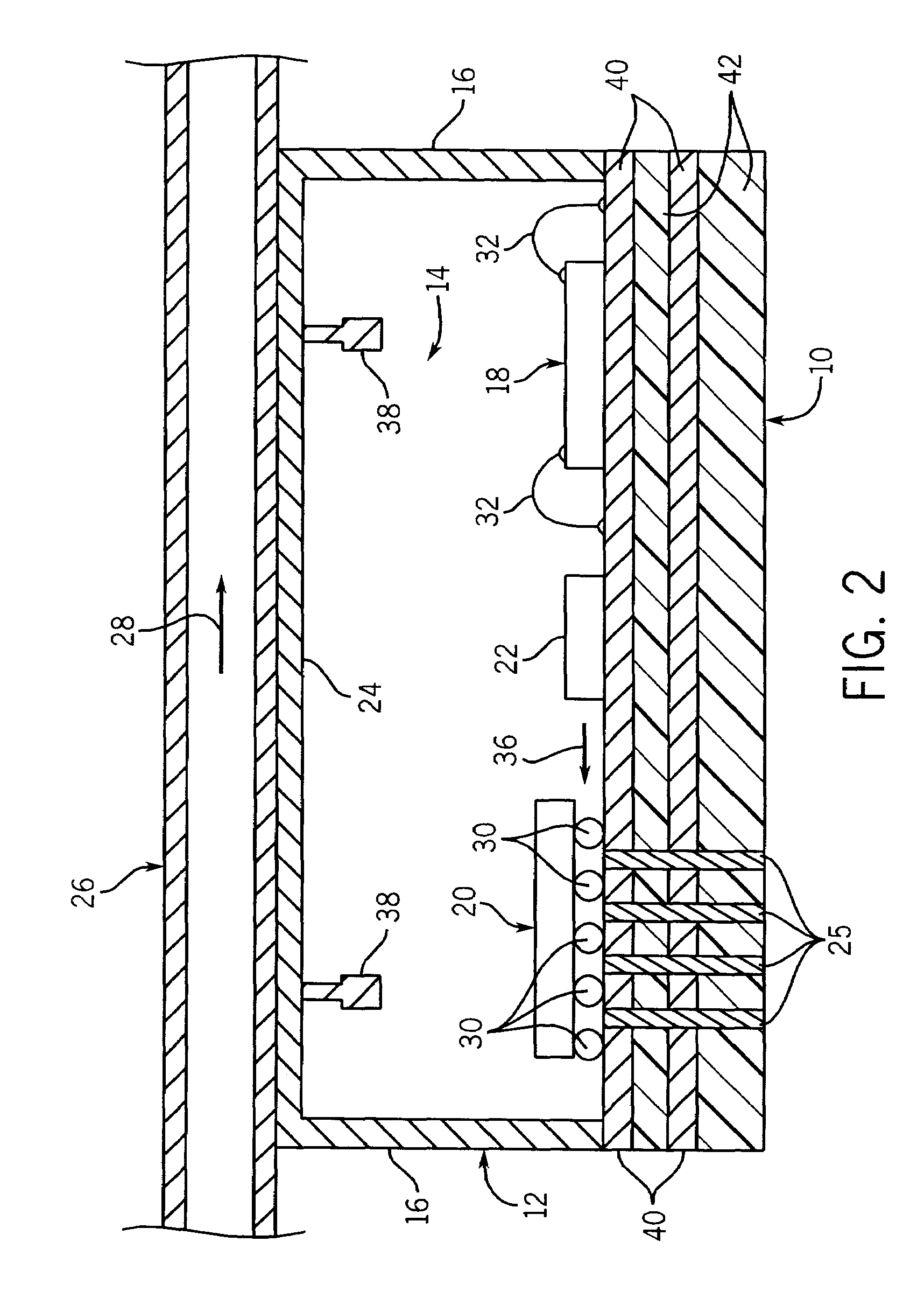
[0013]This invention is a completely self-contained and encapsulated “package” into which a high power integrated circuit (“chip”) such as an amplifier, or an entire subsystem (such as a radar “transmit-receive” module), can be installed to provide the necessary thermal and electrical environment to assure that the chip or multi-chip subsystem works correctly. The packaging approach not only assures that DC electrical power will be delivered to the chip(s) and AC signals will be brought into and led from the chip(s) in a correct manner, but also that the operating temperature of the chip(s) will remain below their maximum survivable operating temperature. This is accomplished by filling the package with a non-electrically conductive working fluid (or mixture) that is above its critical point. The primary package containing the chip(s) and a working fluid are completely hermetically sealed, and in the preferred embodiment the entire cooling process is a transfer of heat from the sour...


PUM


Abstract

A package for a semiconductor chip or other heat producing device has a supporting substrate to which the devices mount and electrically connect. An enclosure is formed over the heat producing devices and filled with a supercritical fluid that transports heat from the devices to a heat sink in thermal contact with the enclosure.

Description

CROSS-REFERENCE TO RELATED APPLICATIONS[0001]This application is based on U.S. Provisional Patent Application Ser. No. 60 / 655,558, filed on Feb. 2, 2005, and entitled “COOLING MECHANISM FOR SELF-CONTAINED INTEGRATED CIRCUIT USING A REVERSIBLE ENDOTHERMIC CHEMICAL REACTION” and U.S. Provisional Patent Application Ser. No. 60 / 632,917, filed Dec. 3, 2004 and entitled “PACKAGING FOR HIGH POWER INTEGRATED CIRCUITS USING SUPERCRITICAL FLUID.”BACKGROUND OF THE INVENTION[0002]The field of the invention is the packaging of electronic devices such as semiconductors, and particularly, the cooling of such devices.[0003]Modern digital and analog integrated circuits (“chips”) are consuming ever-larger amounts of DC power as the number of transistors per unit area is increased in digital chips, and as the amount of output power required of analog chips (such as power amplifiers) is increased through the use of improved design techniques, more capable transistors, and new transistor materials (in t...

Claims


Application Information

Patent Timeline
Patent Type & Authority Patents(United States)
IPC IPC(8): H01L23/46H01L21/44
CPCH01L23/22H01L23/3677H01L23/427H01L2924/00014H01L2224/45014H01L2924/14H01L2924/12041H01L2924/1305H01L2924/1461H01L2924/10253H01L24/48H01L2224/48227H01L2224/48091H01L2224/16225H01L2924/00H01L2224/0401H01L2224/45015H01L2924/207H01L2924/00011H01L2924/206
Inventor WILKINS, WENDY L.GILBERT, BARRY K.KLINE, BRUCE R.
Owner MAYO FOUND FOR MEDICAL EDUCATION & RES
Why Eureka
Try Eureka