

Device for ESD protection circuit
a protection circuit and metal oxide semiconductor technology, applied in the direction of semiconductor devices, electrical equipment, transistors, etc., can solve the problems of abnormal operation of electronic products, damage to most electronic devices or systems, and affect the circuit function of ics, so as to achieve significant enhancement of esd tolerance
- Summary
- Abstract
- Description
- Claims
- Application Information
AI Technical Summary
Benefits of technology
Problems solved by technology
Method used
Image

Examples
Embodiment Construction
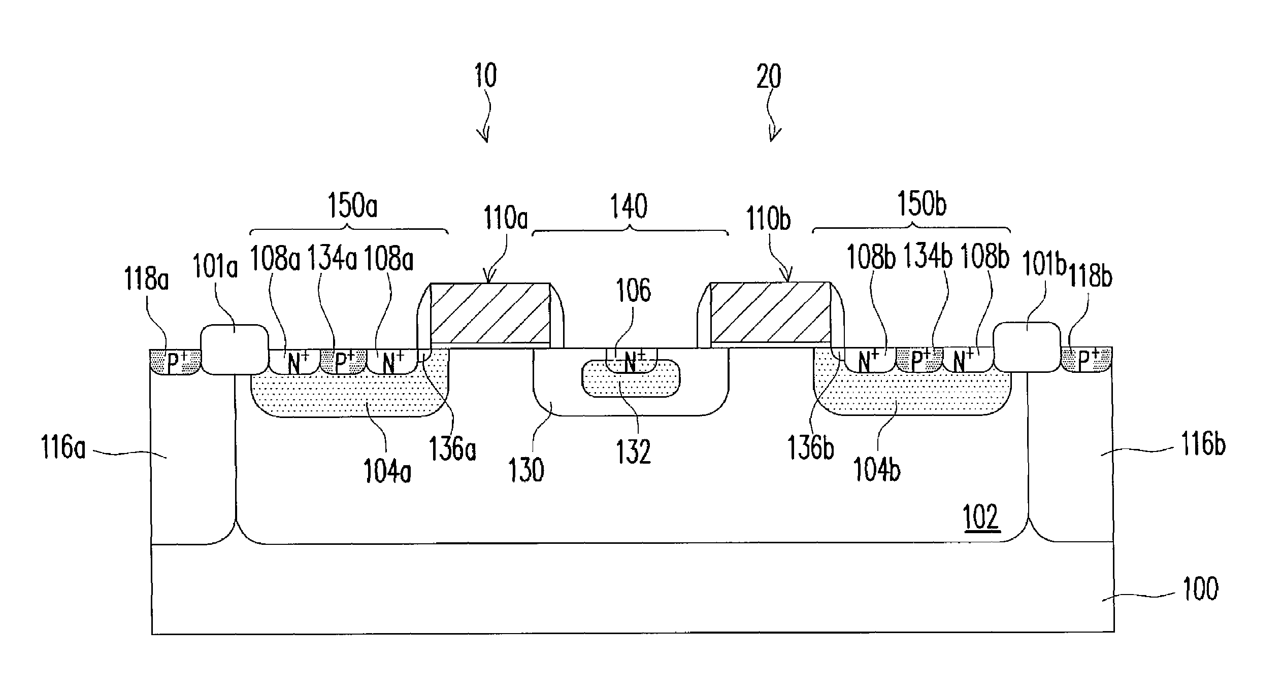
[0032]In the present invention, a LDMOS device for an ESD protection circuit can be a LDNMOS device or a LDPMOS device. In the following embodiments, a LDNMOS device in which the first conductivity type is P-type and the second conductivity type is N-type is provided for illustration purposes, and is not to be construed as limiting the scope of the present invention. It is appreciated by persons skilled in the art that the first conductivity type can be N-type and the second conductivity type can be P-type so as to form a LDPMOS device.
[0033]A device for an ESD protection circuit including two LDNMOS devices is provided for illustration purposes, and is not to be construed as limiting the present invention. The number of the LDMOS devices for the ESD protection circuit is not limited by the present invention.
[0034]FIG. 1 schematically illustrates a cross-section view of a LDNMOS device for an ESD protection circuit according to an embodiment of the present invention.
[0035]Referring ...
PUM
 Abstract
Description
Claims
Application Information