Method and system for parallel processing of IC design layouts

Inactive Publication Date: 2010-02-02
CADENCE DESIGN SYST INC
View PDF68 Cites 11 Cited by
  • Summary
  • Abstract
  • Description
  • Claims
  • Application Information

AI Technical Summary

Benefits of technology

[0004]PV tools read and manipulate a design database which stores information about device geometries and connectivity. Because compliance with design rules generally constitutes the gating factor between one stage of the design and the next, PV tools are typically executed multiple times during the evolution of the design and contribute significantly to the project's critical path. Therefore, reducing PV tool execution time makes a major contribution to the reduction of overall design cycle times.
[0005]As the quantity of data in modern IC designs become larger and larger over time, the execution time required to process EDA tools upon these IC designs also becomes greater. For example, the goal of reducing PV tool execution time is in sharp tension with many modern IC designs being produced by electronics companies that are constantly increasing

Problems solved by technology

Violating a single foundry rule can result in a silicon product that does not work for its intended purpose.
For example, the goal of reducing PV tool execution time is in sharp tension with many modern IC designs being produced by electronics companies that are constantly increasing in complexity and number of transistors.
The more transistors and other structures on an IC design, the greater amounts of time that is normally needed to perform PV processing.
This problem is exacerbated for all EDA tools by constantly improving IC manufacturing technologies that can create IC

Method used


Image

  • Method and system for parallel processing of IC design layouts
  • Method and system for parallel processing of IC design layouts
  • Method and system for parallel processing of IC design layouts

Examples


Example

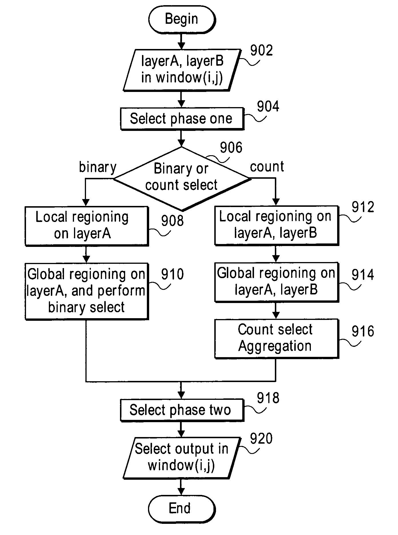
[0031]Disclosed is an improved method and system for implementing parallelism for execution of electronic design automation (EDA) tools, such as layout processing tools. An example of an EDA layout processing tool is a physical verification (PV) tool. To illustrate embodiments of the invention, the below description is made with respect to parallelism for PV tools. It is noted, however, that the present invention is not limited to PV tools, and may also be applied to other types of EDA layout processing tools.

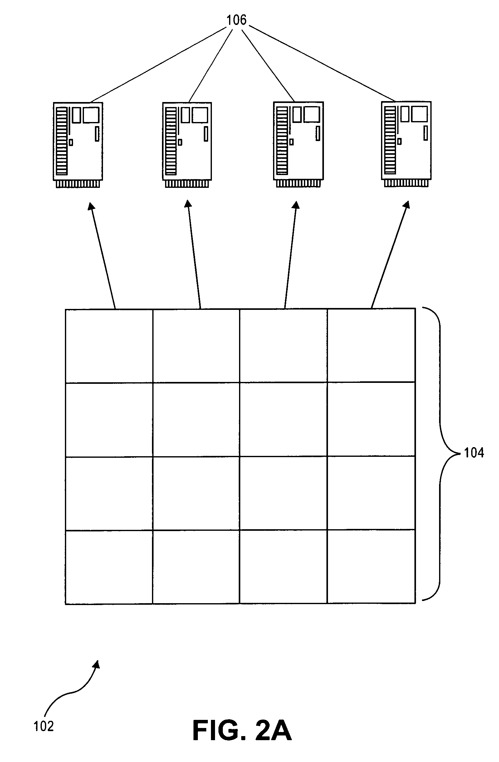
[0032]According to some embodiments of the present invention, parallelism is implemented whereby the design layout is cut into multiple layout portions, and some or all of the layout portions are processed independently on different processing entities. Non-limiting examples of a processing entity includes a processor, a network node, or a CPU in a multi-CPU system.

[0033]Embodiments of the present invention provide a new approach for handling parallel processing for global oper...


PUM


Abstract

Disclosed is a method and system for processing the tasks performed by an IC layout processing tool in parallel. In some approaches, the IC layout is divided into a plurality of layout portions and one or more of the layout portions are processed in parallel, where geometric select operations are performed in which data for different layout portions may be shared between different processing entities. One approach includes the following actions: select phase one operation for performing initial select actions within layout portions; distributed regioning action for local regioning; distributed regioning action for global regioning and binary select; count select aggregation for count-based select operations; and select phase two operations for combining results of selecting of internal shapes and interface shapes.

Description

BACKGROUND AND SUMMARY[0001]The invention relates to the design and manufacture of integrated circuits, and more particularly, to systems and methods for performing physical verification during the circuit design process.[0002]The electronic design process for an integrated circuit (IC) involves describing the behavioral, architectural, functional, and structural attributes of an IC or electronic system. Design teams often begin with very abstract behavioral models of the intended product and end with a physical description of the numerous structures, devices, and interconnections on an IC chip. Semiconductor foundries use the physical description to create the masks and test programs needed to manufacture the ICs.[0003]A Physical Verification (PV) tool is a common example of an EDA tool that is used by electronics designers. PV is one of the final steps that is performed before releasing an IC design to manufacturing. Physical verification ensures that the design abides by all of t...

Claims


Application Information

Patent Timeline
IPC IPC(8): G06F17/50
CPCG06F17/5081G06F30/398
Inventor KOSHY, MATHEWRUEHL, ROLANDCAO, MINMA, LI-LINGCADOURI, EITANZHANG, TIANHAO
Owner CADENCE DESIGN SYST INC
Why Eureka
Try Eureka