
Plasma display panel and method for driving same

a technology of display panel and plasma, which is applied in the direction of gas discharge vessel/container, electric discharge tube, instruments, etc., can solve the problems of shortened ac-pdp life, inferior quality of grown layers compared to those formed, etc., and achieve the effect of shortening the response delay tim

Inactive Publication Date: 2010-02-09
SAMSUNG SDI CO LTD
View PDF22 Cites 5 Cited by
  • Summary
  • Abstract
  • Description
  • Claims
  • Application Information

AI Technical Summary

Benefits of technology

The present invention provides a plasma display panel (PDP) that can shorten response delay time by using extremely pure MgO to form a protective layer on the dielectric layer to prevent unstable discharge based on temperature. The panel includes a first substrate and a second substrate, address electrodes, a first dielectric layer, barrier ribs, a phosphor layer, sustain electrodes, a second dielectric layer, and a protective layer. The method includes determining the temperature of the panel, applying a voltage that gradually decreases from a first voltage to a second voltage to the first electrodes, and sustaining application of the second voltage to the first electrode in a first period of a reset period, wherein the first period is varied according to the temperature of the panel. The technical effect is to improve the response time of the plasma display panel.

Problems solved by technology

However, such grown layers tend to have inferior qualities compared to those formed using a thin film fabrication process.
Therefore, there is a problem in that the dielectric layer and the electrode under the dielectric layer may be damaged by sputtering of electrons and ions generated from the discharge and thus the life-span of the AC-PDP may be shortened.

Method used


Image

  • Plasma display panel and method for driving same
  • Plasma display panel and method for driving same
  • Plasma display panel and method for driving same

Examples


example 1

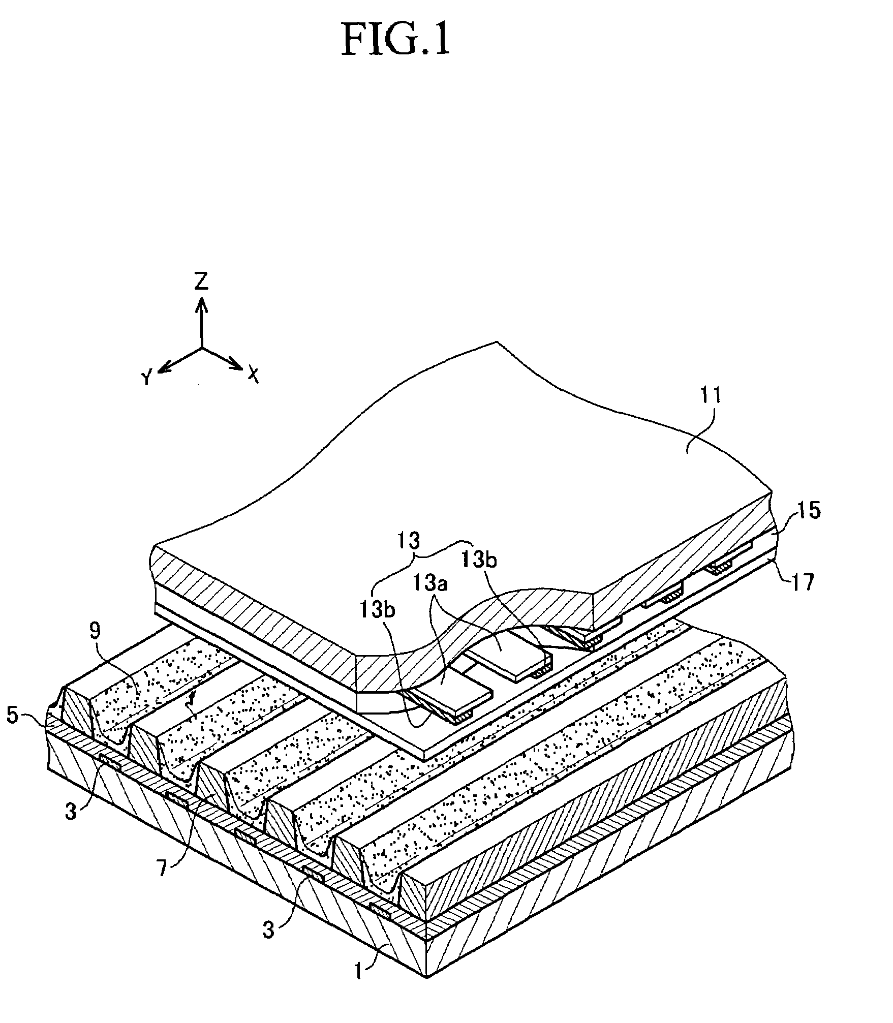
[0047]Stripe-type sustain electrodes were formed of an indium tin oxide conductive material on an upper substrate formed of soda lime glass using a conventional sustain electrode forming method.

[0048]A dielectric layer was then formed over the sustain electrodes and on the upper substrate by coating the entire surface of the upper substrate with a lead-based glass paste and baking the upper substrate.

[0049]An upper panel was prepared by forming a protective layer of a MgO compound on the dielectric layer by using a sputtering method. The MgO compound was prepared through a sintering process, and had a purity of at least 99.6% by weight. The impurities of the MgO compound are revealed in Table 1 below.

example 2

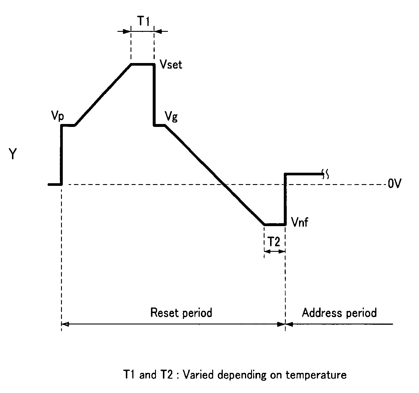
[0050]The same process as in Example 1 was carried out, except that the waveforms of FIGS. 3 and 4 were applied to the plasma display panel prepared in accordance with Example 1.


PUM


Abstract

Provided are a plasma display panel (PDP) and a driving method thereof. The PDP includes a first substrate and a second substrate disposed in parallel and spaced apart from one another. Address electrodes are provided on the first substrate with a first dielectric layer over the address electrodes and the first substrate. Barrier ribs are provided on the dielectric forming a plurality of discharge spaces in which phosphor layers are provided. Sustain electrodes are formed on the second substrate facing the first substrate and are arranged crossing the address electrodes. A second dielectric layer is formed over the address electrodes and on the second substrate, and a protective layer including MgO of at least 99.6% purity by weight is formed over the second dielectric layer by a sintering process. The discharge can be stabilized by varying a Vset applying time or a Vnf voltage applying time according to the temperature of the plasma display panel, and wall charges can be sufficiently accumulated in the reset period.

Description

CROSS-REFERENCE TO RELATED APPLICATION[0001]This application claims priority to and the benefit of Korean Patent Application No. 10-2005-0091051 filed in the Korean Intellectual Property Office on Sep. 29, 2005, the entire content of which is incorporated herein by reference.BACKGROUND OF THE INVENTION[0002]1. Field of the Invention[0003]The present invention relates to a plasma display panel (PDP) and a method for driving the same.[0004]2. Description of the Related Art[0005]A plasma display panel (PDP) is a flat display device using a plasma phenomenon, which is also called a gas-discharge phenomenon since a discharge is generated in the panel when a potential is applied to two electrodes separated from each other under a gas atmosphere in a non-vacuum state. Such a gas discharge phenomenon is used to display an image. Basically, a PDP has a matrix structure where electrodes are provided on opposing substrates and arranged to cross and face each other, and further including a disc...

Claims


Application Information

Patent Timeline
Patent Type & Authority Patents(United States)
IPC IPC(8): G09G3/28G09G3/20G09G3/292G09G3/288G09G3/291G09G3/296G09G3/298H01J11/22H01J11/24H01J11/34H01J11/40
CPCG09G3/2927H01J11/12H01J11/40G09G2310/066G09G2320/041G09G3/296
Inventor KIM, KI-DONGPARK, YONG-SU
Owner SAMSUNG SDI CO LTD
Learn More