Semiconductor device

a technology of semiconductors and solder balls, applied in the direction of electrical apparatus construction details, sustainable manufacturing/processing, final product manufacturing, etc., can solve the problem of insufficient technique, and achieve the effect of enhancing the resistance to cracking of solder balls, enhancing the connection strength of solder balls and reducing the cracking ra

Inactive Publication Date: 2010-02-09
LONGITUDE LICENSING LTD
View PDF6 Cites 10 Cited by
  • Summary
  • Abstract
  • Description
  • Claims
  • Application Information

AI Technical Summary

Benefits of technology

[0012]According to the semiconductor device, the resistance against cracking of solder balls can be enhanced. Thereby, the connection strength of the solder balls and the reliability of a secondary mounting of the semiconductor device can be enhanced.

Problems solved by technology

However, the connection strength is enhanced to some extent, but still not enough in the technique since only the connection strength of conventional NSMD structures can be achieved by the solder resist being shifted to expose the side surface of the land.

Method used


Image

  • Semiconductor device
  • Semiconductor device
  • Semiconductor device

Examples


first embodiment

[0028]Hereinafter, the present invention is explained.

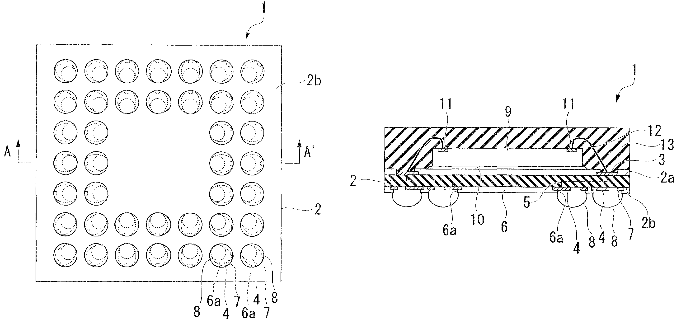
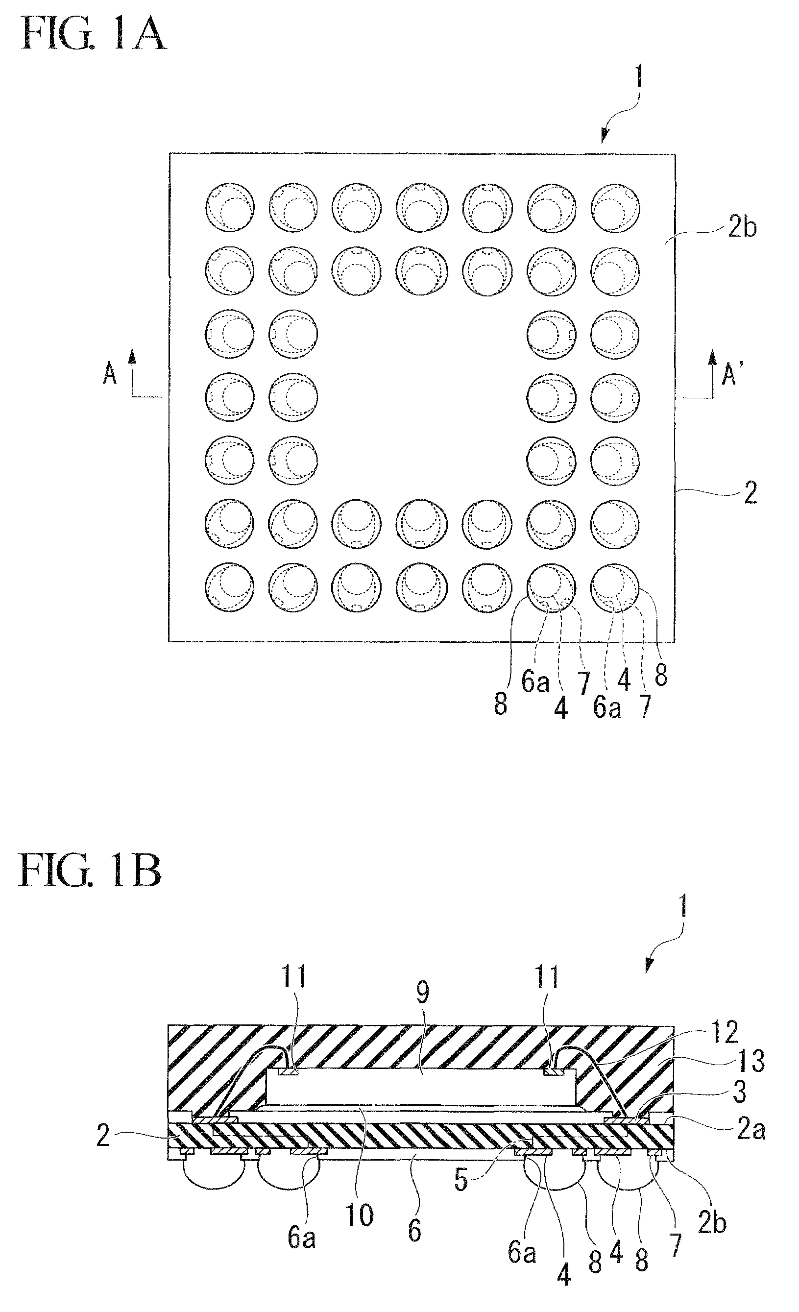
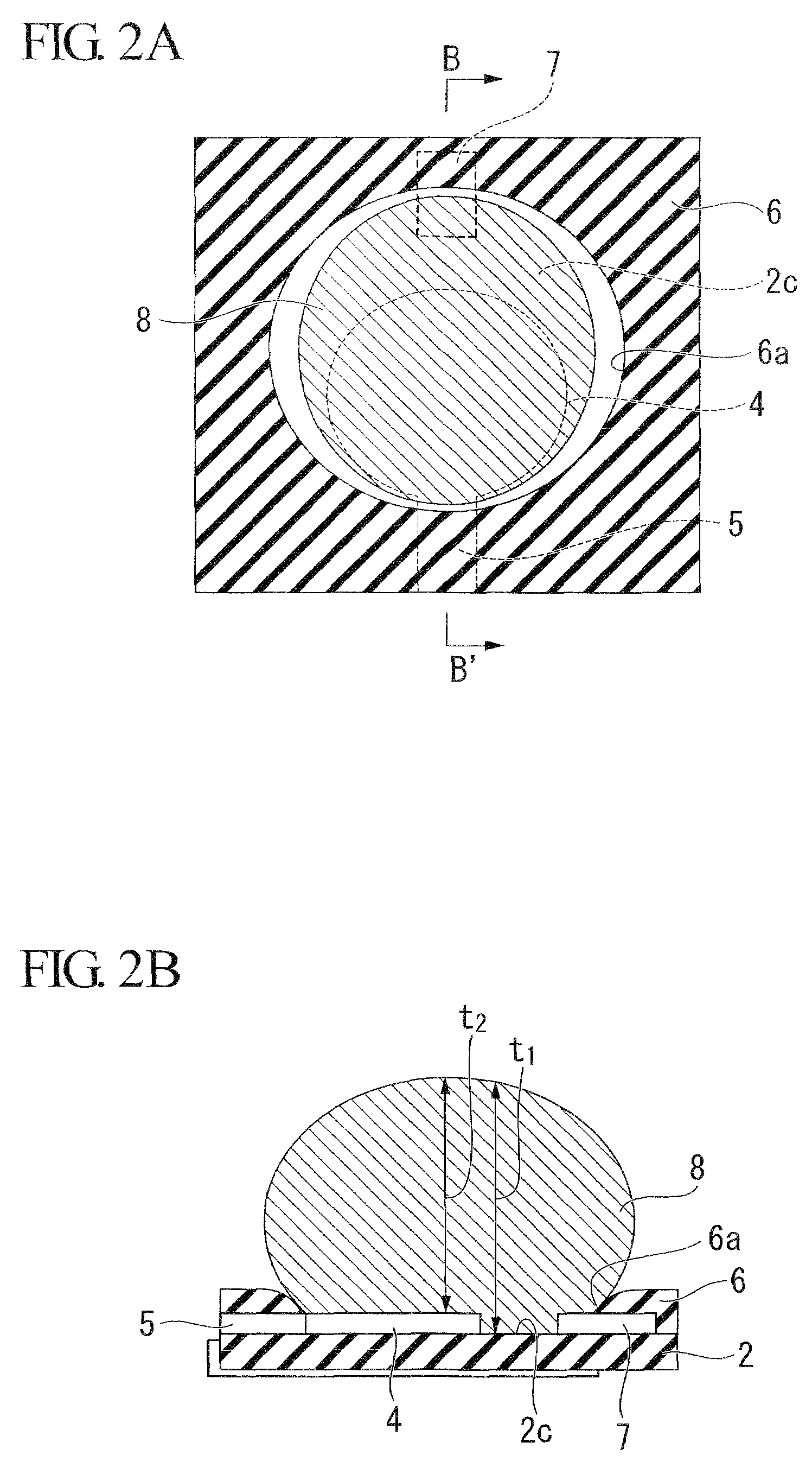
[0029]FIG. 1A is a plane view showing the structure of external terminals of a BGA-type semiconductor device 1 according to the first embodiment of the present invention. FIG. 1B is a cross-sectional view taken along a line A-A′ shown in FIG. 1A. FIG. 2A is a plane view showing the land structure of the semiconductor device 1. FIG. 2B is a cross-sectional view taken along a line B-B′ shown in FIG. 2A.

[0030]As shown in FIG. 1A, the semiconductor device 1 includes a wiring substrate 2 in substantially a rectangular shape, on which wirings are provided. The wiring substrate 2 is, for example, a glass epoxy substrate of 0.25 mm on which wirings are provided. As shown in FIG. 1B, multiple connection pads 3 are provided on the top surface 2a of the wiring substrate 2. Multiple lands 4 are provided in a grid on the bottom surface of the wiring substrate 2. The lands 4 are electrically connected to the corresponding connection pads 3 by ...

second embodiment

[0049]Hereinafter, the present invention is explained.

[0050]FIG. 5 is a cross-sectional view showing the land structure of a semiconductor device 1A according to the second embodiment of the present invention. To further enhance the reliability with respect to portions of a wiring substrate 2A and a mounting substrate 14A on which damage is focused, the thickness of a solder resist 6 on the circumference of a land 4A is arbitrarily changed so that the solder resist 6B on the side of a portion on which stress is focused becomes thinner than the solder resist 6A, for example. As a result, the solder ball 8 is shifted because of the difference in the thicknesses of the solder resists 6A and 6B. Thereby, the thickness of the portion on which damage is focused can be thicker. As a result, the resistance against cracking increases, and the reliability of the entire package can be enhanced. The thickness of the solder resist can be adjusted by providing asperity to a jig used for planariza...

third embodiment

[0051]Hereinafter, the present invention is explained.

[0052]FIG. 6 is a plane view showing the land structure of a semiconductor device 1B according to the third embodiment of the present invention. As shown in FIG. 6, multiple dummy wirings 7B are provided so that the connection area of the wiring substrate 2B and the solder ball is further increased.


PUM


Abstract

A semiconductor device includes: a wiring substrate including multiple connection pads provided on a top surface thereof and multiple lands that are provided on a bottom surface thereof and electrically connected to the corresponding connection pads; a semiconductor chip mounted on the top surface of the wiring substrate and electrically connected to the connection pads; a solder resist deposited on the bottom surface of the wiring substrate and having multiple openings to which the lands are respectively exposed, each of the openings being shifted with respect to a corresponding land of the lands; multiple external terminals connected respectively to the lands through the openings; and a dummy wiring arranged on the bottom surface of the wiring substrate and separately from the corresponding land so that a corresponding external terminal of the external terminals is connected to the corresponding land and the dummy wiring partially exposed to the corresponding opening.

Description

BACKGROUND OF THE INVENTION[0001]1. Field of the Invention[0002]The present invention relates to a semiconductor device formed by a semiconductor chip being mounted on a package substrate, and to an electronic device including the semiconductor device.[0003]Priority is claimed on Japanese Patent Application No. 2007-321751, filed Dec. 13, 2007, the content of which is incorporated herein by reference.[0004]2. Description of the Related Art[0005]Recently, greater miniaturization and multi-layering of wirings have been progressing with the higher integration of semiconductor chips. On the other hand, miniaturization of the package size is required for high-density packaging of a semiconductor package (semiconductor device). For example, a semiconductor package, such as BGA (ball grid array) and CSP (chip size package), has a structure in which a semiconductor chip is mounted on a package substrate, and the semiconductor chip and the package substrate are connected using, for example, ...

Claims


Application Information

Patent Timeline
Patent Type & Authority Patents(United States)
IPC IPC(8): H05K7/02H05K7/06H05K7/08H05K7/10
CPCH01L21/561H01L23/3128H01L23/49816H01L23/49838H01L24/10H01L24/97H05K1/111H01L24/13H01L24/28H01L24/45H01L24/48H01L24/85H01L2224/13099H01L2224/45124H01L2224/45144H01L2224/45147H01L2224/48091H01L2224/48228H01L2224/73265H01L2224/85201H01L2224/85205H01L2224/97H01L2924/01004H01L2924/01013H01L2924/01029H01L2924/01038H01L2924/01079H01L2924/07802H01L2924/15311H05K2201/09663H05K2201/09781H05K2201/0989H05K2201/10734H01L2924/01006H01L2224/32225H01L2224/48227H01L2924/01005H01L2924/01019H01L2924/01033H01L2924/181H01L24/73H01L2224/13Y02P70/611H01L2924/00014H01L2224/85H01L2224/83H01L2224/92247H01L2924/00H01L2924/3512H01L2924/00012Y02P70/50
Inventor FUJII, SEIYA
Owner LONGITUDE LICENSING LTD
Why Eureka
Try Eureka