Supercharge Your Innovation With Domain-Expert AI Agents!

Method of testing a sequential access memory plane and a corresponding sequential access memory semiconductor device

a semiconductor device and sequential access technology, applied in the direction of electronic circuit testing, static storage, measurement devices, etc., can solve the problems of substantial hardware implementation and “routability” of the connection between the components, and achieve the effect of small overall size of the test logic and simple implementation

Active Publication Date: 2010-02-09
STMICROELECTRONICS SRL
View PDF8 Cites 0 Cited by
  • Summary
  • Abstract
  • Description
  • Claims
  • Application Information

AI Technical Summary

Benefits of technology

[0004]The invention aims to address the above mentioned problems. An object of the invention is to provide a sequential access memory array test that allows a particularly simple implementation leading to an extremely small overall size of the test logic.
[0006]In other words, unlike the conventional prior art tests, in which the n bits of an extracted test word are compared simultaneously and in parallel with an expected data word, the sequential bit-by-bit comparison of each extracted word in accordance with the invention enables the use of extremely simple comparison logic, for example including an EXCLUSIVE OR or EXCLUSIVE NOR logic gate.
[0007]In one embodiment of the method, the p test words each of n bits are written in such a way as to obtain a checkerboard test binary configuration in the memory plane. The expected data is obtained sequentially from respective logical combinations of the read addresses of the test words and the ranks of the test bits in each word that is read. This kind of embodiment makes it extremely simple to generate the expected data.

Problems solved by technology

Also, in addition to this penalizing aspect of the overall surface area, this kind of decoder logic causes substantial problems with the hardware implementation (“routability”) of the connections between the components of the decoder logic.

Method used


Image

  • Method of testing a sequential access memory plane and a corresponding sequential access memory semiconductor device
  • Method of testing a sequential access memory plane and a corresponding sequential access memory semiconductor device
  • Method of testing a sequential access memory plane and a corresponding sequential access memory semiconductor device

Examples


Embodiment Construction

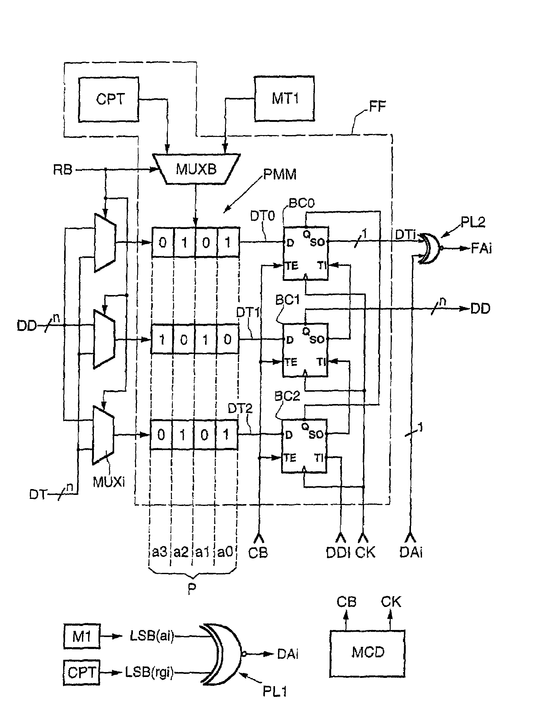
[0018]FIG. 1 shows a sequential access memory device FF, for example an FIFO memory. The memory FF includes a memory array PMM able to store p words each of n bits. In other words, the depth of the memory is equal to p and the width of the data bus is equal to n. In the example described here, for simplicity, p=4 and n=3. The figure shows the successive storage addresses ai of the p words in the memory array PMM.

[0019]In the normal operating mode writing and reading are effected in the conventional manner using write and read pointers controlled in the conventional manner by control circuit / means CPT. A multiplexer MUXB controls the write and read pointers of the memory array in response to a control signal RB from either the control means CPT (in the normal mode of operation) or the test mode control circuit / means MT1 (in the test mode of operation). Similarly, the data to be written into the memory array is selected via n multiplexers MUXi which are also controlled by the control ...


PUM


Abstract

The sequential access memory array is able to store p words each of n bits. Such p test words each made up of n test bits are written in the memory array, the p test words are extracted sequentially and, for each current word extracted, the n test bits that compose it are compared sequentially with n respective expected data bits before extracting the next test word.

Description

FIELD OF THE INVENTION[0001]The invention concerns sequential access memories, in particular first in / first out (FIFO) memories, and especially testing such memories, using a dedicated test circuit integrated during fabrication of the memory and the associated test algorithm.BACKGROUND OF THE INVENTION[0002]At present, a test circuit integrated into a memory and an associated test algorithm, known to the person skilled in the art as a built-in self-test (BIST) algorithm, write dedicated test words into the memory array on command and then extract them and compare the test bits of the extracted words with the expected binary data bits. This necessitates the use of decoder logic which is connected to the output of the memory array and also receives the expected data, whose overall size increases as the width of the data bus of the memory increases, i.e. as the number of bits of the test words increases.[0003]Also, in addition to this penalizing aspect of the overall surface area, this...

Claims


Application Information

Patent Timeline
Patent Type & Authority Patents(United States)
IPC IPC(8): G11C29/00G01R31/28G11C29/38
CPCG11C29/003G11C29/38
Inventor BEAUJOIN, MARCALOFS, THOMASARMAGNAT, PAUL
Owner STMICROELECTRONICS SRL
Features
  • R&D
  • Intellectual Property
  • Life Sciences
  • Materials
  • Tech Scout
  • Unparalleled Data Quality
  • Higher Quality Content
  • 60% Fewer Hallucinations
Learn More