Logic compatible arrays and operations

a logic and array technology, applied in the field of memory cells and arrays, multipletimes programming memory structure and manufacturing methods, can solve the problems of reducing the performance of the most advanced standard logic process, not only increasing the wafer cost, so as to reduce the size of memory cells, reduce program disturbance, and reduce the effect of page-wise erasur

Active Publication Date: 2010-02-16
TAIWAN SEMICON MFG CO LTD
View PDF18 Cites 13 Cited by
  • Summary
  • Abstract
  • Description
  • Claims
  • Application Information

AI Technical Summary

Benefits of technology

[0015]The advantageous features of the present invention include reduced memory cells size, reduced program disturb and the ability for page-wise erasing.

Problems solved by technology

Integrating MTP-specific process steps into the standard CMOS-based logic process creates complications.
This prior approach not only increases the wafer cost, but it also falls short of the peak performance that the most advanced standard logic process can deliver.
In addition, high voltages adversely causes program disturbance to other rows and columns.
This results in an increase in the size of the memory cells.

Method used


Image

  • Logic compatible arrays and operations
  • Logic compatible arrays and operations
  • Logic compatible arrays and operations

Examples


Embodiment Construction

[0023]The making and using of the presently preferred embodiments are discussed in detail below. It should be appreciated, however, that the present invention provides many applicable inventive concepts that can be embodied in a wide variety of specific contexts. The specific embodiments discussed are merely illustrative of specific ways to make and use the invention, and do not limit the scope of the invention.

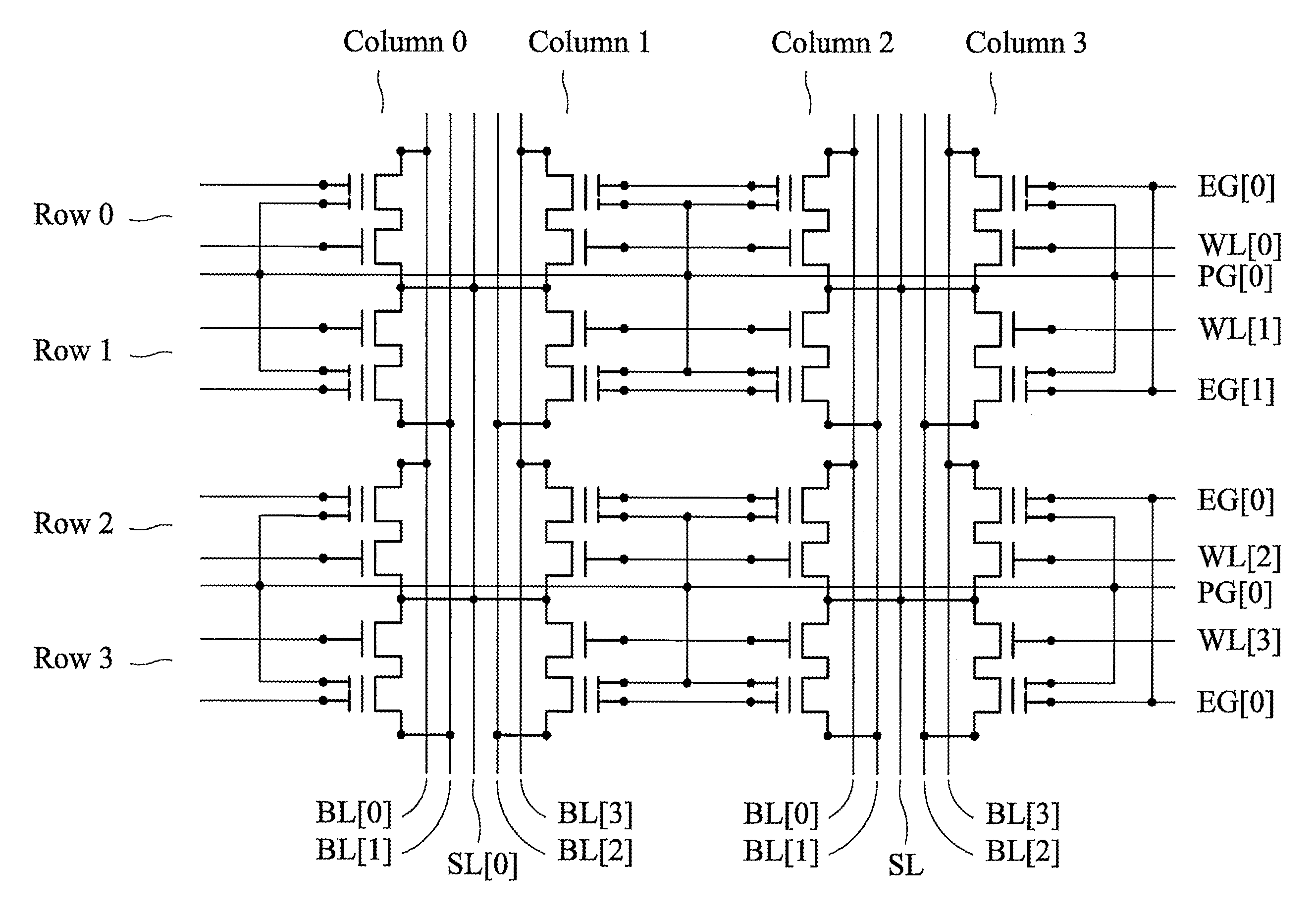
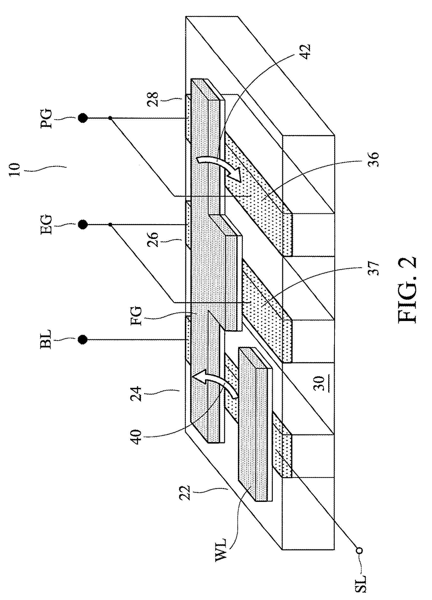
[0024]FIG. 2 illustrates a perspective view of a multiple-times programming (MTP) memory cell 10, which includes transistor 22, first capacitor 24, second capacitor (also referred to as a coupling capacitor) 26, and third capacitor 28. First capacitor 24, second capacitor 26 and third capacitor 28 share a common floating gate FG. Transistor 22 is controlled by word-line WL, which controls the selection of current memory cell 10. Bit-line BL is connected to transistor 22. It is noted that source line SL and bit-line BL are swapped as compared to conventional connections. Coupl...


PUM


Abstract

An array of memory cells arranged in a plurality of rows and a plurality of columns are provided. The array includes a first program line in a first direction, wherein the first program line is connected to program gates of memory cells in a first row of the array; a first erase line in the first direction, wherein the first erase line is connected to erase gates of the memory cells in the first row of the array; and a first word-line in the first direction, wherein the first word-line is connected to word-line nodes of the memory cells in the first row of the array.

Description

CROSS-REFERENCE TO RELATED APPLICATIONS[0001]This application relates to the following co-pending and commonly assigned patent application: Ser. No. 11 / 248,357, filed Oct. 12, 2005, entitled Logic Compatible Non-Volatile Memory Cell, which application is hereby incorporated herein by reference.TECHNICAL FIELD[0002]This invention relates generally to semiconductor devices, and more particularly to memory cells and arrays, and even more particularly to the structure and manufacturing methods of multiple-times programming memory (MTP) cells and arrays.BACKGROUND[0003]A multiple-times programming (MTP) memory cell retains information stored in the memory cell even when the power is turned off. To create a MTP memory cell, typically, a standard CMOS-based logic process is used as a starting foundation. Next, additional process steps are incorporated into the logic process flow to create the MTP memory cell. Examples of such additional process steps include second polysilicon deposition, ...

Claims


Application Information

Patent Timeline
Patent Type & Authority Patents(United States)
IPC IPC(8): G11C11/34
CPCG11C16/0433G11C16/10G11C16/3427H01L27/115H01L27/11521H01L27/11558H10B41/60H10B69/00H10B41/30
Inventor CHIH, YUE-DERHSU, TE-HSUN
Owner TAIWAN SEMICON MFG CO LTD
Why Eureka
Try Eureka