Sense amplifier circuit having current mirror architecture

a technology of amplifier circuit and mirror structure, which is applied in the direction of amplifiers with semiconductor devices/discharge tubes, dc-amplifiers with dc-coupled stages, instruments, etc., can solve the problem that the prior art sense amplifier circuit cannot meet the requirements

Active Publication Date: 2010-02-16
EMEMORY TECH INC
View PDF5 Cites 391 Cited by
  • Summary
  • Abstract
  • Description
  • Claims
  • Application Information

AI Technical Summary

Problems solved by technology

That is to say, if the voltage levels at N3 and N4 are required to be always complemented to each other and be determinate before finishing the latch operation, the aforementioned prior art sense amplifier circuit cannot meet the requirements.

Method used


Image

  • Sense amplifier circuit having current mirror architecture
  • Sense amplifier circuit having current mirror architecture
  • Sense amplifier circuit having current mirror architecture

Examples


Embodiment Construction

[0021]Hereinafter, preferred embodiments of the present invention will be described in detail with reference to the accompanying drawings. Here, it is to be noted that the present invention is not limited thereto.

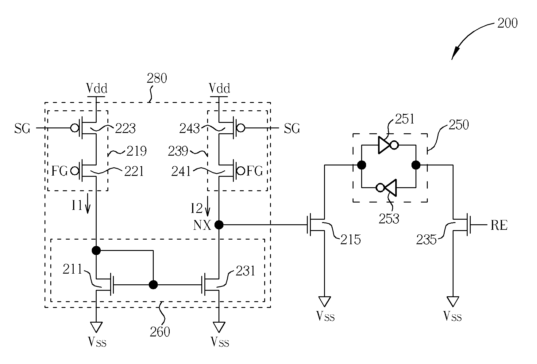
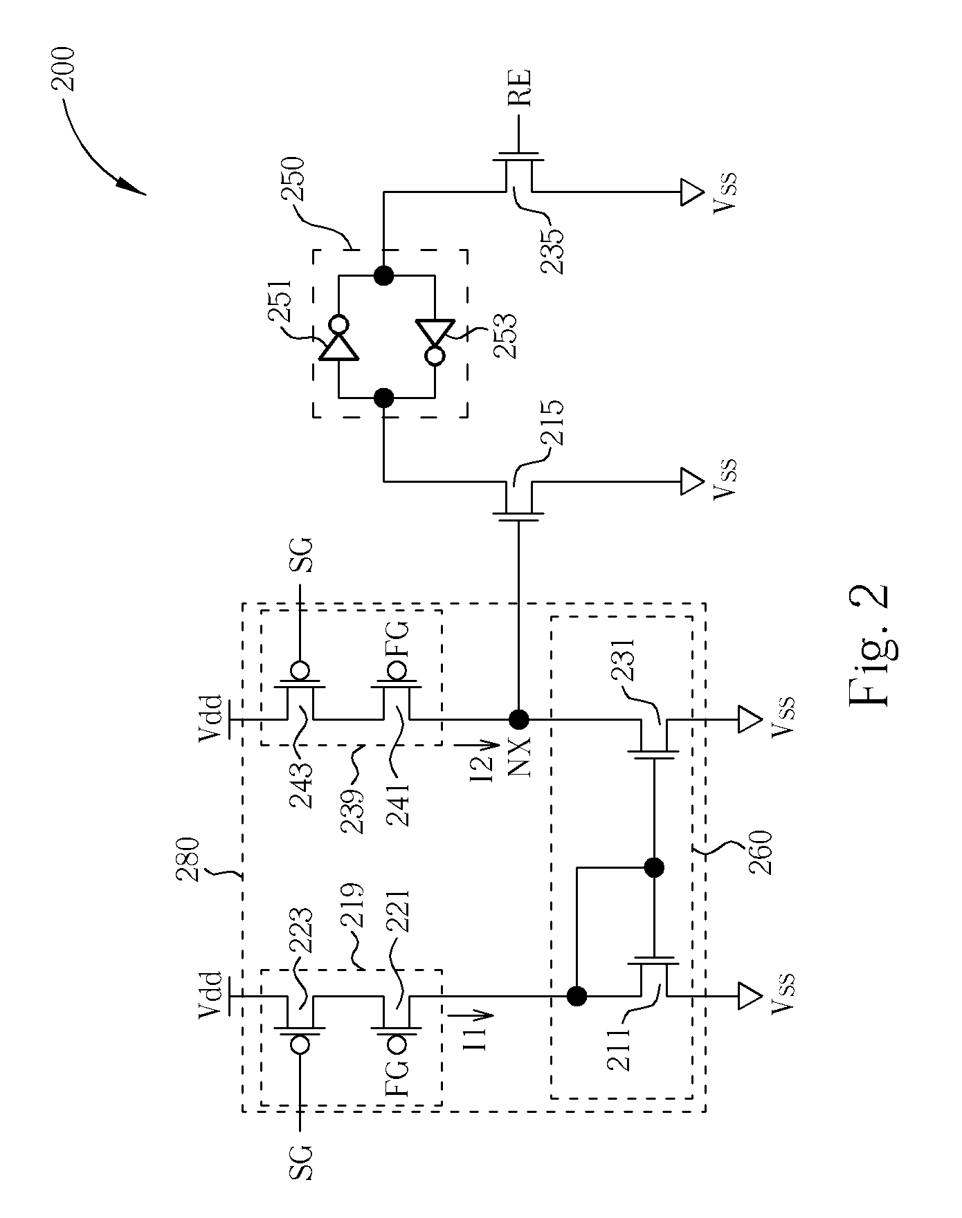
[0022]Please refer to FIG. 2, which is a circuit diagram schematically showing the structure of a sense amplifier circuit 200 in accordance with a first preferred embodiment of the present invention. The sense amplifier circuit 200 comprises a current sensing unit 280, a latch circuit 250, and NMOS transistors 215 and 235. The current sensing unit 280 comprises a current mirror circuit 260, a first non-volatile memory unit 219, and a second non-volatile memory unit 239. The current mirror circuit 260 comprises two NMOS transistors 211 and 231. The first non-volatile memory unit 219 comprises a PMOS transistor 223 and a first non-volatile memory device 221. The second non-volatile memory unit 239 comprises a PMOS transistor 243 and a second non-volatile memory device 241. Th...


PUM


Abstract

A sense amplifier circuit for use in a semiconductor memory device has complemented logic states at opposite sides of the latch circuit in the sense amplifier circuit determinate all the time in operation. The sense amplifier circuit takes advantage of a current mirror circuit for ascending or descending a voltage level at the gate of a transistor by charge accumulation or charge dissipation, which turns on or off the transistor so as to control the logic states at opposite sides of the latch circuit in the sense amplifier circuit.

Description

BACKGROUND OF THE INVENTION[0001]1. Field of the Invention[0002]The present invention relates in general to a sense amplifier circuit, and more particularly, to a sense amplifier circuit having current mirror architecture for semiconductor memory devices.[0003]2. Description of the Prior Art[0004]Since semiconductor memory devices (for example, flash memory, DRAM and SRAM, etc) have always been one of the most important components for electronic appliances, the performance of memory devices is highly demanded and is improving uninterruptedly.[0005]Please refer to FIG. 1, which is a circuit diagram schematically showing the structure of a prior art sense amplifier circuit 100. The sense amplifier circuit 100 comprises a first current sensing unit 110, a second current sensing unit 130, and a latch circuit 150. The first current sensing unit 110 comprises NMOS transistors 111, 113 and 115, a PMOS transistor 117, and a first non-volatile memory unit 119. The second current sensing unit...

Claims


Application Information

Patent Timeline
Patent Type & Authority Patents(United States)
IPC IPC(8): G11C11/34G11C16/06
CPCG11C7/065
Inventor TSAI, HONG-PINGLIN, CHING-YUAN
Owner EMEMORY TECH INC
Why Eureka
Try Eureka