Structures and methods for an application of a flexible bridge

a flexible bridge and structure technology, applied in the field of semiconductor integrated circuits, can solve the problems of increasing power consumption, poor communication performance between chips, and difficulty in aligning chips properly using existing mounting structures, such as conventional single-chip modules or conventional multi-chip modules, and achieve the effect of facilitating high-bandwidth communication

Active Publication Date: 2010-03-02
ORACLE INT CORP
View PDF3 Cites 6 Cited by
  • Summary
  • Abstract
  • Description
  • Claims
  • Application Information

AI Technical Summary

Benefits of technology

[0009]One embodiment of the present invention provides a system that facilitates high-bandwidth communication using a flexible bridge. This system includes a chip with an active face upon which active circuitry and signal pads reside, and a second component with a surface upon which active circuitry and / or signal pads reside. A flexible bridge provides high-bandwidth communication between the active face of the chip and the surface of the second component. This flexible bridge provides a flexible connection that allows the chip to be moved with six degrees of freedom relative to the second component without affecting communication between the chip and the second component. Hence, the flexible bridge allows the chip and the second component to communicate without requiring precise alignment between the chip and the second component.
[0010]In a variation on this embodiment, the system allows signals to be sent between the circuits on the chip and the second component by matching the wire line size in the flexible bridge to the size of circuits and / or signal pads on the chip and the second component, thereby alleviating wireability and bandwidth limitations of conventional chip packaging technologies.
[0018]In a further variation, the flexible bridge comprises multiple layers of metal traces and / or planes separated by dielectrics. An enhanced thermal conductivity layer and / or plane, for instance an additional metal layer, can be used to assist in heat transfer.

Problems solved by technology

Sub-optimal alignment can result in poor communication performance between chips and increased power consumption.
Unfortunately, aligning chips properly using existing mounting structures, such as conventional single-chip modules or conventional multi-chip modules, is not a simple matter.
The chips in these structures are subject to thermal expansion and mechanical vibrations, as well as manufacturing and assembly perturbations that cause alignment problems.
Furthermore, a need to deliver power and cooling to chips that communicate through proximity communication further complicates chip alignment.

Method used


Image

  • Structures and methods for an application of a flexible bridge
  • Structures and methods for an application of a flexible bridge
  • Structures and methods for an application of a flexible bridge

Examples


Embodiment Construction

[0072]The following description is presented to enable any person skilled in the art to make and use the invention, and is provided in the context of a particular application and its requirements. Various modifications to the disclosed embodiments will be readily apparent to those skilled in the art, and the general principles defined herein may be applied to other embodiments and applications without departing from the spirit and scope of the present invention. Thus, the present invention is not limited to the embodiments shown, but is to be accorded the widest scope consistent with the claims.

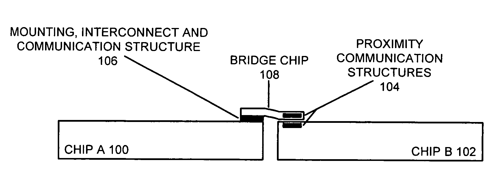
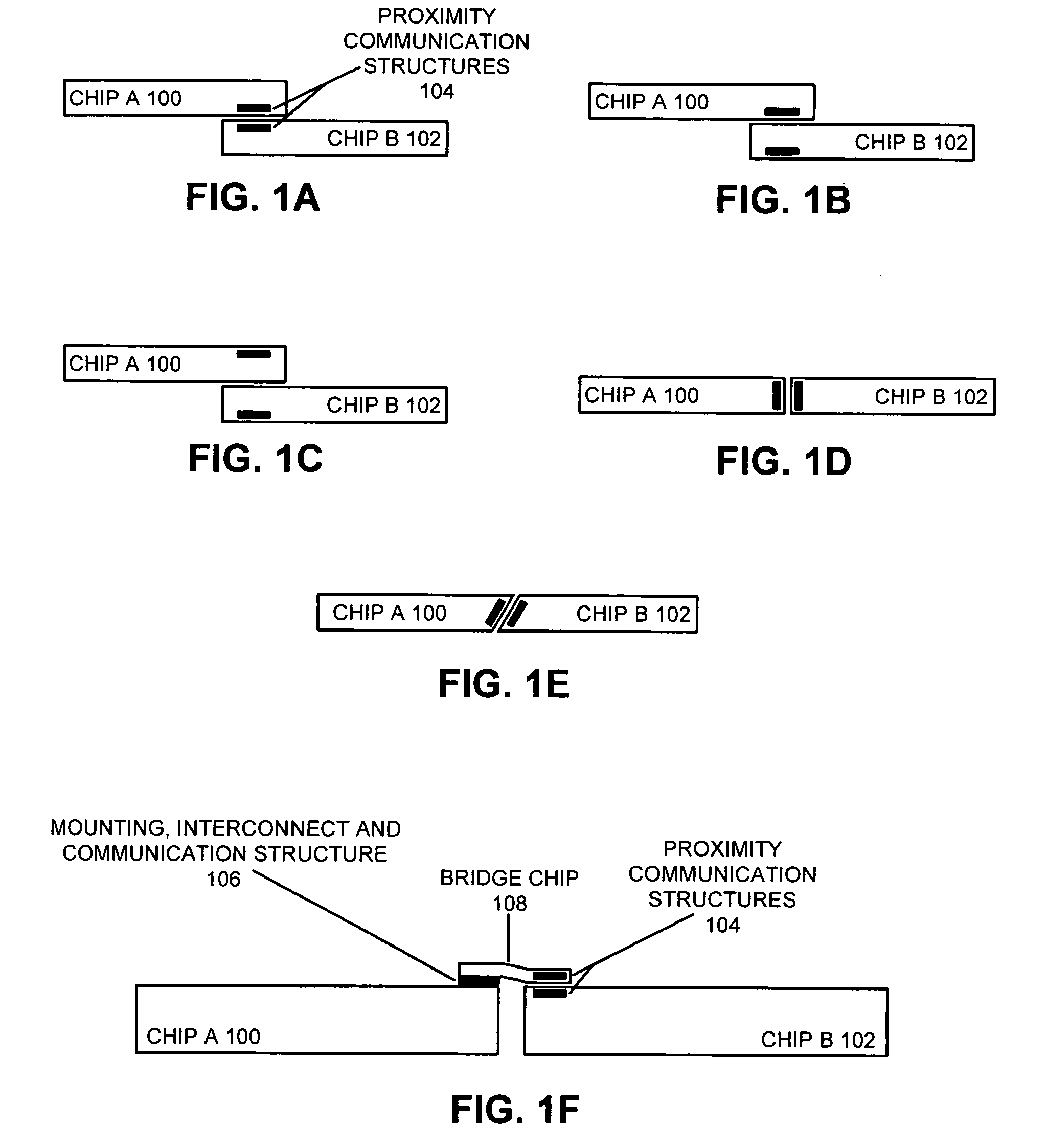
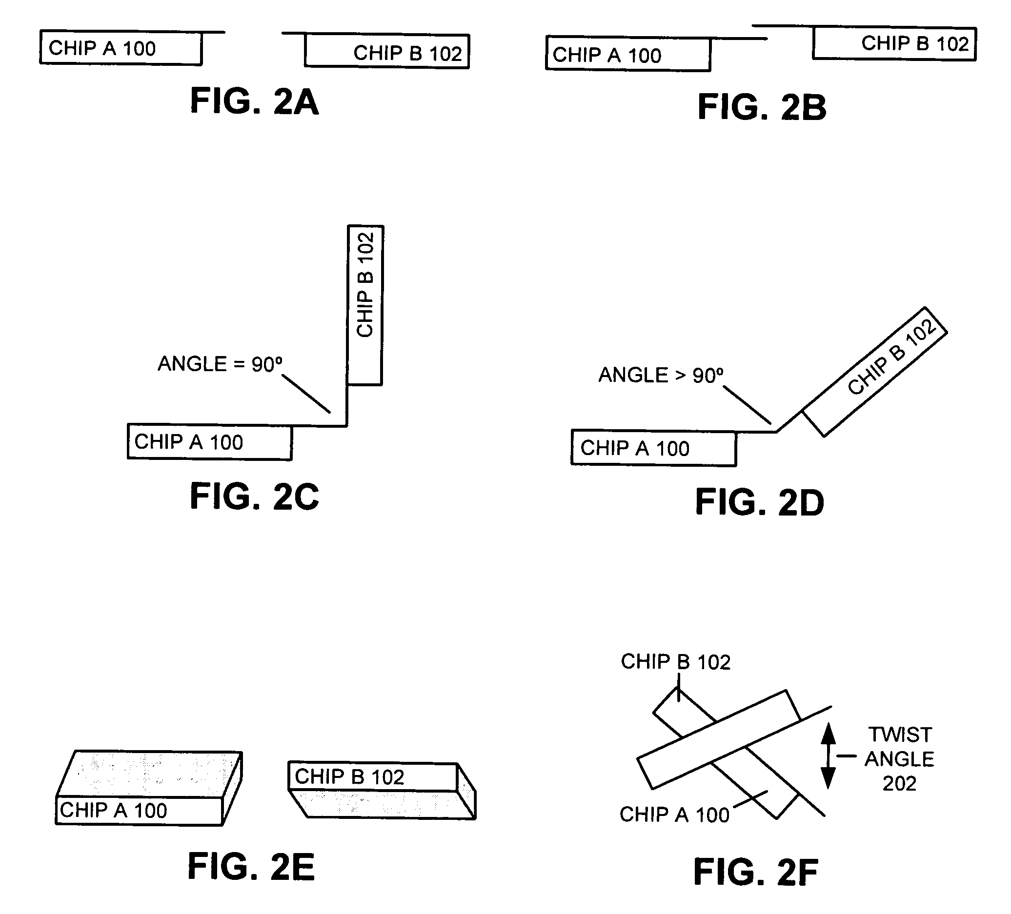
Inter-Chip Bandwidth and Alignment

[0073]Chips in electronic systems are often mounted to single-chip modules (SCMs). The chip and SCM are assembled together, and then each SCM undergoes individual burn-in and testing, after which they can be mounted to a printed-wiring board (PWB) or printed-wiring card (PWC). However, while SCMs provide favorable yield with moderate cost, they also present c...


PUM


Abstract

One embodiment of the present invention provides a system that facilitates high-bandwidth communication using a flexible bridge. This system includes a chip with an active face upon which active circuitry and signal pads reside, and a second component with a surface upon which active circuitry and / or signal pads reside. A flexible bridge provides high-bandwidth communication between the active face of the chip and the surface of the second component. This flexible bridge provides a flexible connection that allows the chip to be moved with six degrees of freedom relative to the second component without affecting communication between the chip and the second component. Hence, the flexible bridge allows the chip and the second component to communicate without requiring precise alignment between the chip and the second component.

Description

RELATED APPLICATION[0001]The subject matter of this application is related to the subject matter in a co-pending non-provisional application by the same inventors as the instant application and filed on the same day as the instant application entitled, “Structures and Methods for a Flexible Bridge that Enables High-Bandwidth Communication,” having Ser. No. 11 / 418,985, and filing date 04 May 2006. This application also claims priority under 35 U.S.C. §119(e) to U.S. Provisional Application Ser. No. 60 / 677,621, filed on 04 May 2005, and to U.S. Provisional Application Ser. No. 60 / 677,585, filed on 4 May 2005, the contents of which are herein incorporated by reference.GOVERNMENT LICENSE RIGHTS[0002]This invention was made with United States Government support under Contract No. NBCH3039002 awarded by the Defense Advanced Research Projects Administration. The United States Government has certain rights in the invention.BACKGROUND[0003]1. Field of the Invention[0004]The present invention...

Claims


Application Information

Patent Timeline
Patent Type & Authority Patents(United States)
IPC IPC(8): H01L39/00H01L21/00
CPCH01L23/48H01L23/5387H01L25/0655H05K3/222H01L2224/16225H01L2225/06562H01L2924/15311H01R12/62H05K2201/1053H05K2201/10674H01L2924/01067
Inventor ZINGHER, ARTHUR R.GUENIN, BRUCE M.HO, RONALDDROST, ROBERT J.
Owner ORACLE INT CORP
Why Eureka
Try Eureka