Dynamic control of back gate bias in a FinFET SRAM cell

a back gate bias and finfet technology, applied in the field of dynamic control of back gate bias, can solve the problems of difficult voltage (vt) control, serious problem of dopant fluctuations, and increased difficulty in vt control

Inactive Publication Date: 2010-03-23
GLOBALFOUNDRIES INC
View PDF9 Cites 132 Cited by
  • Summary
  • Abstract
  • Description
  • Claims
  • Application Information

AI Technical Summary

Problems solved by technology

Dopant fluctuations pose a serious problem in threshold voltage (Vt) control in advanced semiconductor devices, such as static random access memory (SRAM).
As semiconductor devices become smaller and smaller, Vt control becomes more difficult.
One serious problem with this solution is that the use of back gates in semiconductor devices has resulted in increased layout complexity, increased wiring densities, and therefore, higher cost.
Further, known back gate biasing schemes have not been able to provide sufficient stability, performance, and reduction in leakage voltages, especially for SRAM.

Method used


Image

  • Dynamic control of back gate bias in a FinFET SRAM cell
  • Dynamic control of back gate bias in a FinFET SRAM cell
  • Dynamic control of back gate bias in a FinFET SRAM cell

Examples


Embodiment Construction

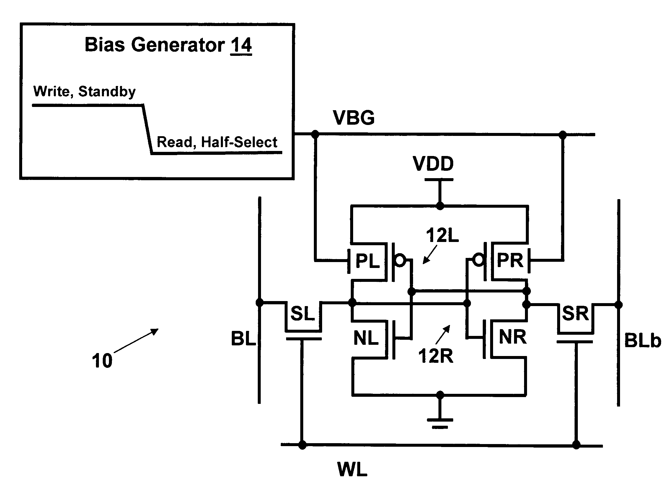
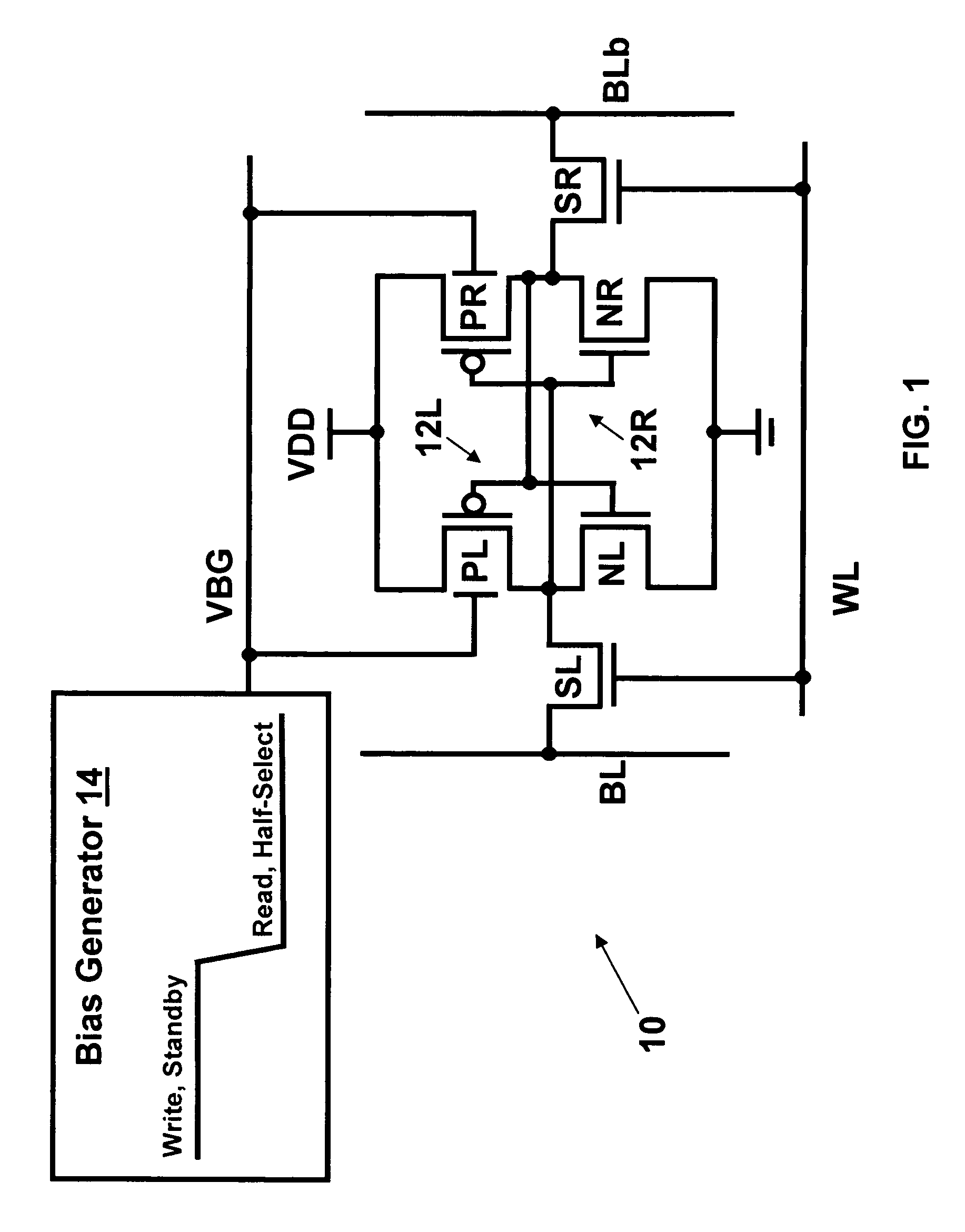
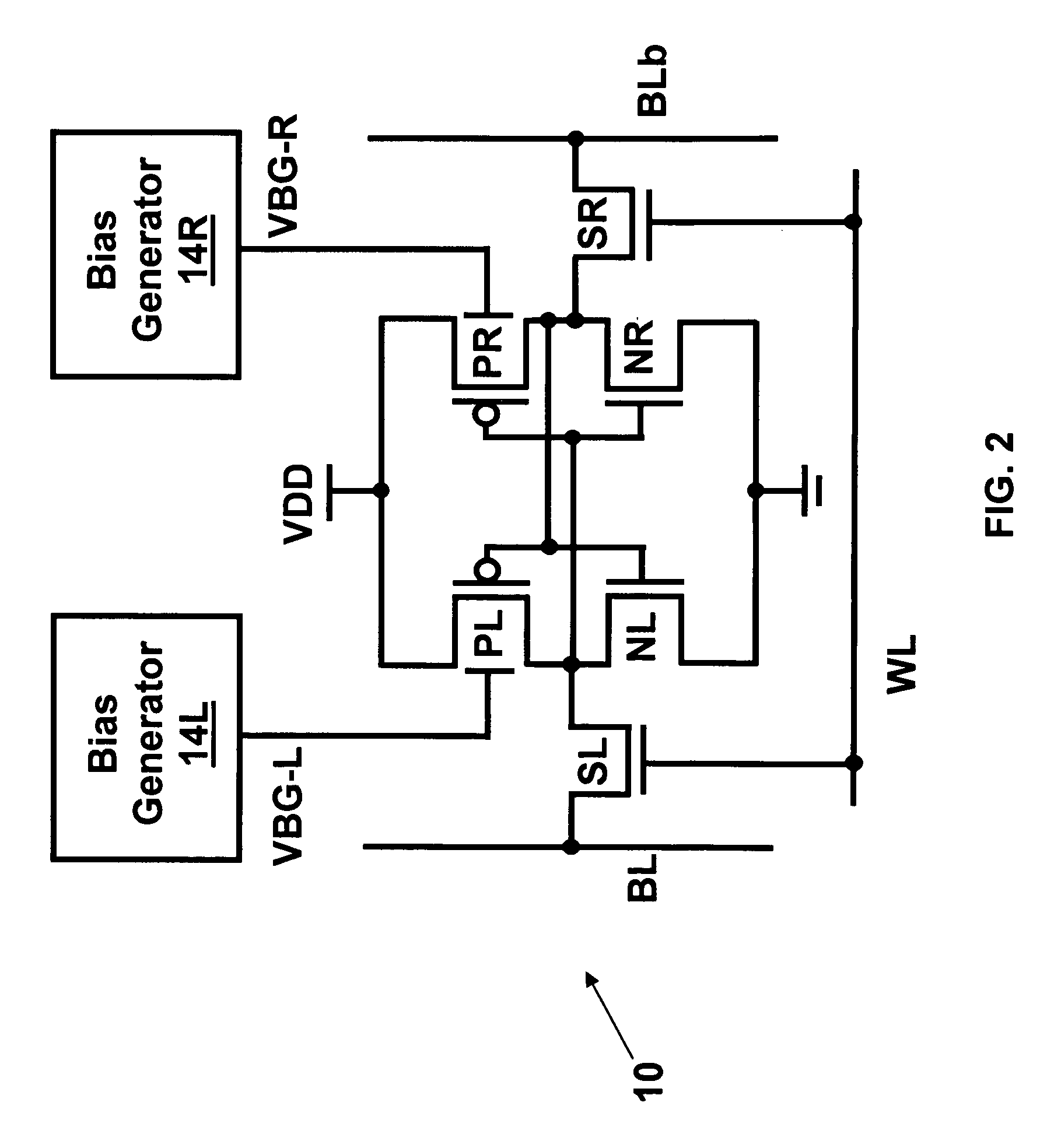
[0021]A 6-T FinFET SRAM cell 10 including dynamic control of back gate bias in accordance with an embodiment of the present invention is depicted in FIG. 1. The SRAM cell 10 includes a pair of cross-coupled inverters 12L, 12R, and a pair of pass nFETs SL and SR connected to bit lines BL and BLb, respectively. The inverter 12L is formed by a pull-down FET NL and a pull-up pFET PL, and the inverter 12R is formed by a pull-down nFET NR and a pull-up pFET PR. A gate of each pass nFET SL and SR is connected to a word line WL.

[0022]The SRAM cell 10 further includes a bias generator 14 for dynamically controlling the bias voltage VBG applied to the back gates of the pFETs PL and PR, based on the operational mode of the SRAM cell 10 (i.e., Read, Half-Select, Write, Standby). The pFETs PL and PR are formed with asymmetrical gates, wherein the gates are formed using different types of polysilicon (n+ or p+) or different gate work functions. Further, the pFETs PL and PR have an independently c...


PUM


Abstract

The present invention provides dynamic control of back gate bias on pull-up pFETs in a FinFET SRAM cell. A method according to the present invention includes providing a bias voltage to a back gate of at least one transistor in the SRAM cell, and dynamically controlling the bias voltage based on an operational mode (e.g., Read, Half-Select, Write, Standby) of the SRAM cell.

Description

FIELD OF THE INVENTION[0001]The present invention relates to semiconductor devices, and more specifically to dynamic control of back gate bias on pull-up pFETs in a FinFET SRAM cell.BACKGROUND OF THE INVENTION[0002]Dopant fluctuations pose a serious problem in threshold voltage (Vt) control in advanced semiconductor devices, such as static random access memory (SRAM). As semiconductor devices become smaller and smaller, Vt control becomes more difficult. A known solution is to use back gates, such as found in FinFETs and other double gate transistors, to control Vt in the semiconductor devices. One serious problem with this solution is that the use of back gates in semiconductor devices has resulted in increased layout complexity, increased wiring densities, and therefore, higher cost. Further, known back gate biasing schemes have not been able to provide sufficient stability, performance, and reduction in leakage voltages, especially for SRAM.SUMMARY OF THE INVENTION[0003]The prese...

Claims


Application Information

Patent Timeline
Patent Type & Authority Patents(United States)
IPC IPC(8): G11C11/00
CPCG11C11/412
Inventor JOSHI, RAJIV V.KIM, KEUNWOONOWAK, EDWARD J.WILLIAMS, RICHARD Q.
Owner GLOBALFOUNDRIES INC
Why Eureka
Try Eureka