Non-volatile memory array architecture with joined word lines

a memory array and non-volatile technology, applied in the field of semiconductor memories, can solve the problems of slow memory array access time due to word line resistance, inability to make metal straps the same width as ultra narrow word lines, and difficulty in locating metal straps for small geometry memory arrays with narrow width word lines. , to achieve the effect of lowering resistance, increasing width, and speeding up word line speed

Active Publication Date: 2010-03-23
ATMEL CORP
View PDF13 Cites 35 Cited by
  • Summary
  • Abstract
  • Description
  • Claims
  • Application Information

AI Technical Summary

Benefits of technology

[0007]In another embodiment, pairs of joined word lines are associated with a single row decoder. With two word lines associated with a single row decoder, the number of row decoders is reduced.

Problems solved by technology

In the prior art, the problem of slow memory array access time due to word line resistance has been recognized.
For example, see U.S. Pat. No. 6,266,264 to R. Proebsting. However, it is not possible to make metal straps the same width as the ultra narrow word lines and so a problem exists in locating metal straps for small geometry memory arrays having narrow width word lines.
This approach has been used in several variations but does not appear suitable where word lines have the minimum feature size, F, as a width dimension.

Method used


Image

  • Non-volatile memory array architecture with joined word lines
  • Non-volatile memory array architecture with joined word lines
  • Non-volatile memory array architecture with joined word lines

Examples


Embodiment Construction

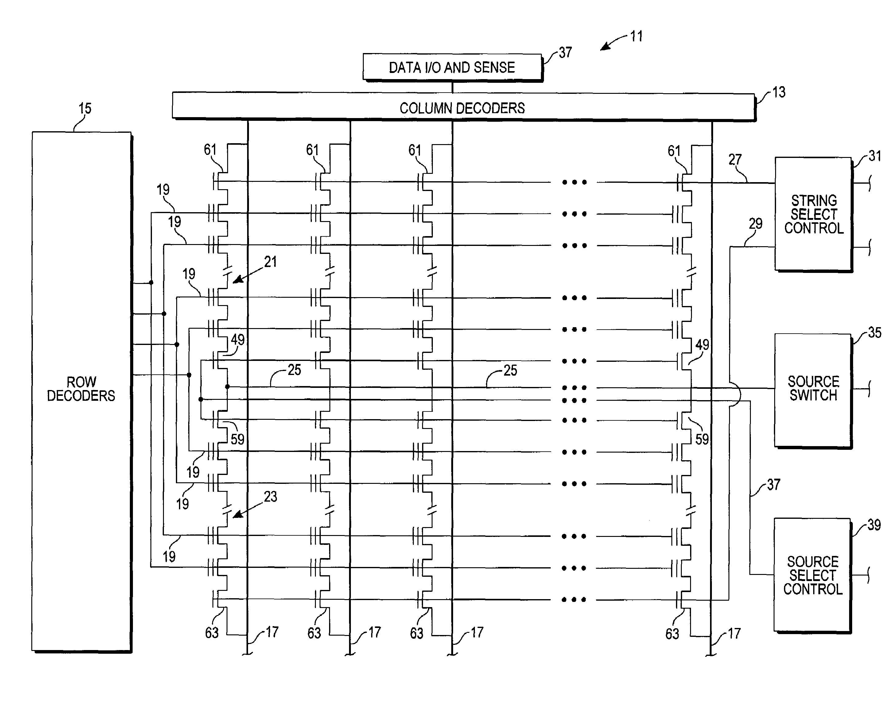
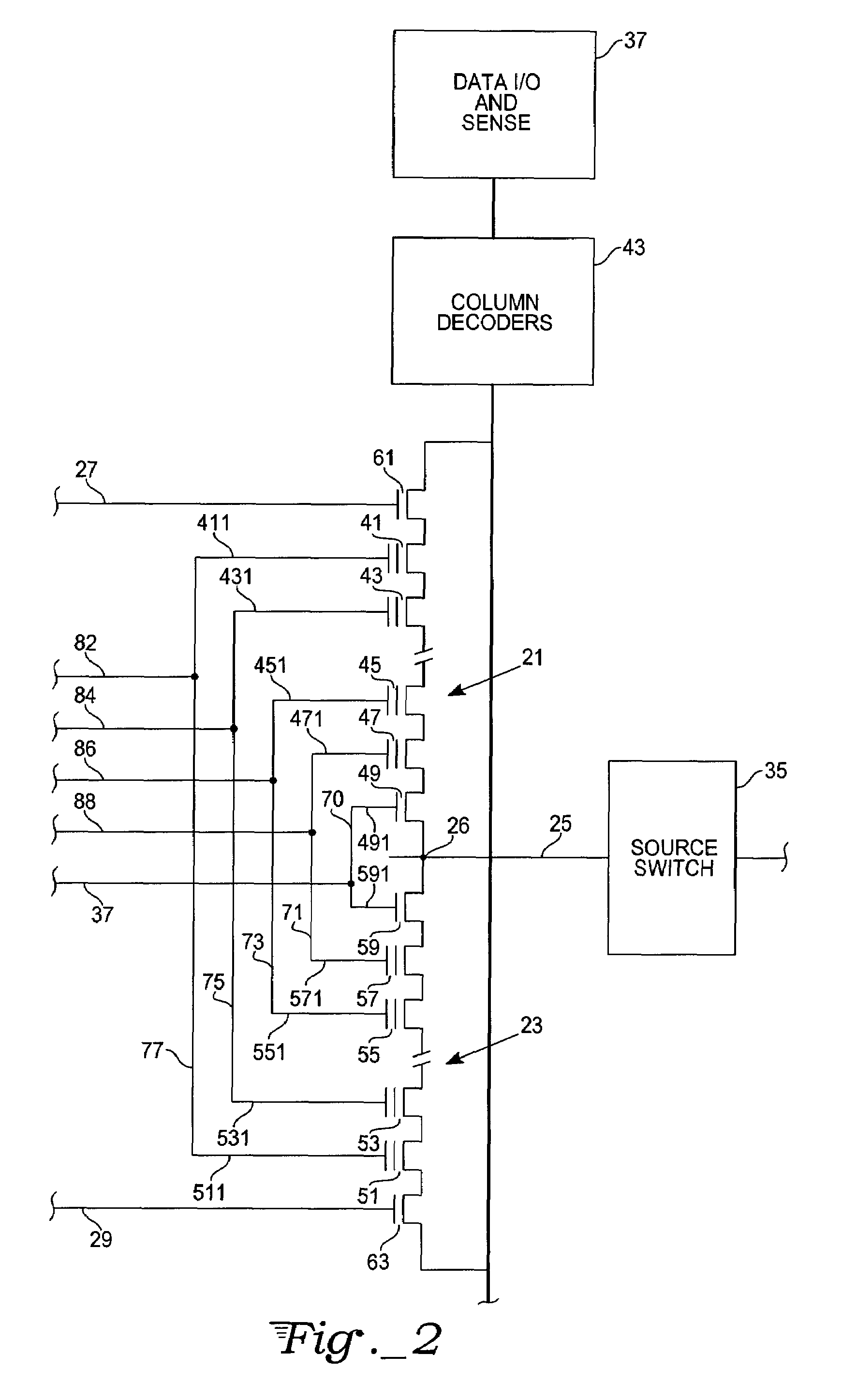
[0019]With reference to FIG. 1, a portion of a non-volatile NAND memory array 11 has column decoders 13 and row decoders 15. The array portion 11 is a left portion of a symmetric memory array having a mirror image right portion described below with reference to FIG. 8. The mirror image portion may share the same column and row decoders. The memory array portion 11 has bit lines 17 associated with the column decoders and with select transistors 61 and 63 for each string of the non-volatile array. Since the memory array 11 is a NAND array, the source of one memory cell is connected to the drain of an adjacent cell in a cascaded string arrangement where each string has a number of transistors representing one byte. In the exemplary embodiment of FIG. 1, two strings connected together hold two strings of data. More than two strings could be cascaded. A first string 21 in the non-volatile array is in cascade relationship with the second string 23 with the source line 25 running between t...


PUM

PropertyMeasurementUnit
program voltageaaaaaaaaaa
feature size widthaaaaaaaaaa
widthaaaaaaaaaa

Abstract

In an embodiment, a non-volatile memory array wherein narrow word lines, as small as the minimum feature size width F, in separate strings, are extended outwardly from a non-volatile memory array and joined by wider connector segments. The joined word lines provide new opportunities. First, metal straps that can be formed to overlie the word lines can be joined by metal connector segments to the word lines. The connector segments can serve as an interface between the polysilicon word lines and the metal straps. Two adjacent word lines in the same string share a single metal strap using these segments thereby reducing the overall number of segments and contacts in the array. Increased width of the polysilicon joinder segments joining word lines in different strings, provides the opportunity for widening the connection beyond the minimum feature size so that contact may be readily made between the metal straps and the polysilicon word lines. Second, the joined word lines require fewer row decoder circuits. One row decoder is provided for each joined set of word lines.

Description

TECHNICAL FIELD[0001]The invention relates to semiconductor memories and, in particular, to non-volatile memory arrays.BACKGROUND ART[0002]In semiconductor non-volatile memory arrays, word lines and bit lines are usually arranged in rows and columns, respectively, to address memory cells. Word lines and bit lines either span the entire array or large blocks of memory cells in the array. Address decoders formed of row decoders and column decoders select appropriate word lines and bit lines to program, read and erase memory cells. Bit lines are usually associated with subsurface source-drain electrodes, while word lines are usually associated with top level select gates of non-volatile memory transistors.[0003]As non-volatile memory cell size shrinks, the smallest memory cells can have a dimension of F, the minimum feature size, or perhaps slightly larger such as 2F or 3F, when viewed in top view. As a specific dimension, F depends on lithographic equipment, but is scalable to whateve...

Claims


Application Information

Patent Timeline
Patent Type & Authority Patents(United States)
IPC IPC(8): G11C11/34G11C16/04G11C5/06
CPCG11C16/3418Y10T29/49002
Inventor SCHUMANN, STEVEFRULIO, MASSIMILIANOBARTOLI, SIMONEBEDARIDA, LORENZOHUI, EDWARD SHUE-CHING
Owner ATMEL CORP
Why Eureka
Try Eureka