Front-end processed wafer having through-chip connections

a technology of through-chip connections and processed wafers, which is applied in the field of semiconductor/solid-state device testing/measurement, individual semiconductor device testing, instruments, etc., can solve the problem that the back end processing for adding metal interconnect layers has not been completed, and achieve the effect of reducing risk and cos

Active Publication Date: 2010-03-30
CUFER ASSET LTD LLC
View PDF263 Cites 24 Cited by
  • Summary
  • Abstract
  • Description
  • Claims
  • Application Information

AI Technical Summary

Benefits of technology

[0006]We have devised a way to minimize the risk and cost associated with the use of through-chip electrical connections in conjunction with device-bearing chips.
[0007]With one type of implementation, involving forming the through-chip connections on a blank wafer, the risk of damaging devices is advantageously eliminated (because there are no devices to damage). Moreover, in the event of a problem that renders the wafer unusable, the cost effect is also reduced because the wafer has not yet undergone any device creation or back-end processing procedures.
[0008]Another type of implementation, involves forming the through chip connections on a wafer where the devices have been formed, but the back end processing to add the metal interconnect layers has not been completed. With this implementation approach, transistors that may be very sensitive to processing and need flat and extremely defect-free areas can be formed without the risk of contamination, thereby improving transistor yield while still obtaining the routing benefits because the vias can be formed before the first metal layer is deposited during a back-end process, after the first metal layer is deposited but before the second metal layer is deposited, or more generally, before depositing of any of the “n” layers that may be deposited as part of the back-end processing.

Problems solved by technology

Another type of implementation, involves forming the through chip connections on a wafer where the devices have been formed, but the back end processing to add the metal interconnect layers has not been completed.
For instance, some of these advantages are mutually contradictory, in that they cannot be simultaneously present in a single embodiment.

Method used


Image

  • Front-end processed wafer having through-chip connections
  • Front-end processed wafer having through-chip connections
  • Front-end processed wafer having through-chip connections

Examples


Embodiment Construction

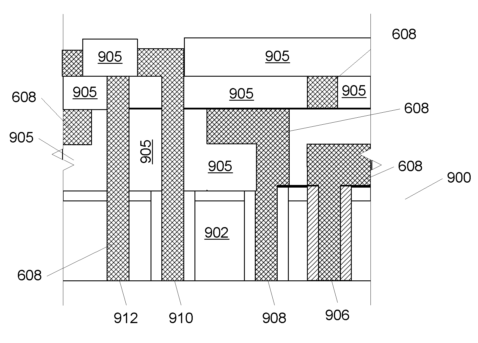
[0019]U.S. patent application Ser. Nos. 11 / 329,481, 11 / 329,506, 11 / 329,539, 11 / 329,540, 11 / 329,556, 11 / 329,557, 11 / 329,558, 11 / 329,574, 11 / 329,575, 11 / 329,576, 11 / 329,873, 11 / 329,874, 11 / 329,875, 11 / 329,883, 11 / 329,885, 11 / 329,886, 11 / 329,887, 11 / 329,952, 11 / 329,953, 11 / 329,955, 11 / 330,011, 11 / 556,747 and 11 / 422,551, incorporated herein by reference describe various techniques for forming small, deep vias in, and electrical contacts for, semiconductor wafers. Our techniques allow for via densities and placement that was previously unachievable and can be performed on a chip or wafer scale.

[0020]In cases where it is desirable to create through-chip electrical connections, but minimize the risks involved with fully processed wafers (i.e. device bearing wafers), the following approach can be used.

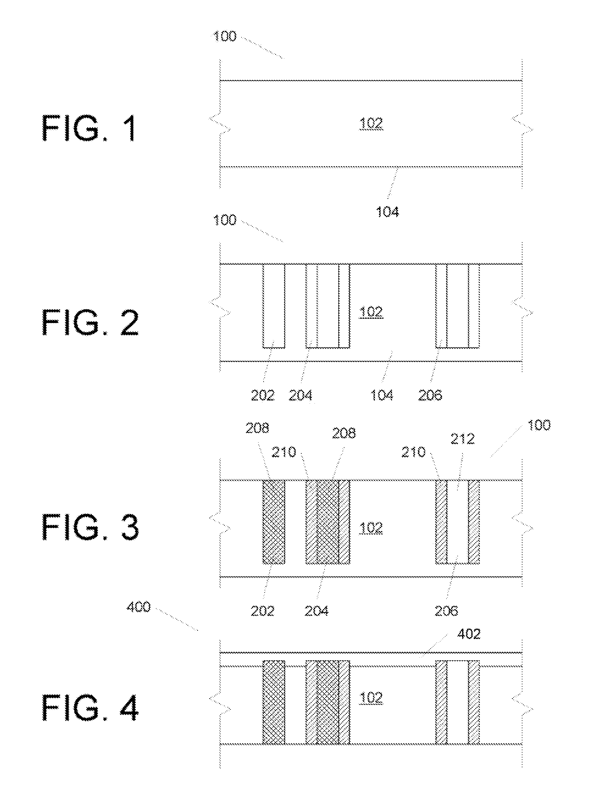
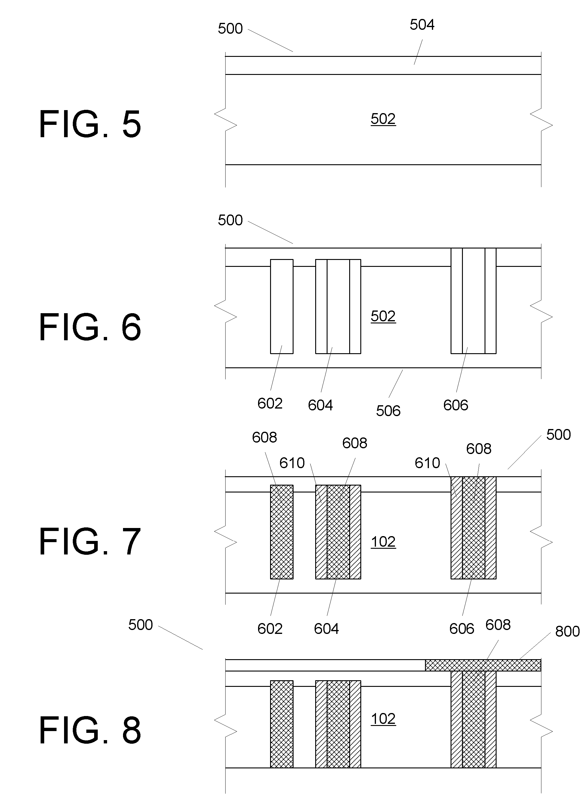
[0021]In summary overview, the approach straightforwardly involves forming vias in a blank wafer at the locations where they should be relative to devices that would be on the wafer once front...


PUM


Abstract

A method involves forming vias in a device-bearing semiconductor wafer, making at least some of the vias in the device-bearing semiconductor wafer electrically conductive, and performing back-end processing the device-bearing semiconductor wafer so as to create electrical connections between an electrically conductive via and a metallization layer. An alternative method involves forming vias in a device-bearing semiconductor wafer, making at least some of the vias in the device-bearing semiconductor wafer electrically conductive, and processing the device-bearing semiconductor wafer so as to create electrical connections between an electrically conductive via and a conductive semiconductor layer.

Description

CROSS REFERENCE TO RELATED APPLICATIONS[0001]This application claims the benefit of priority, pursuant to 35 U.S.C. 119(e), of U.S. Provisional Application Ser. No. 60 / 882,671 filed Dec. 29, 2006, and is also a continuation-in-part of U.S. patent application Ser. No. 11 / 422,551 filed Jun. 6, 2006, the entirety of which are all are incorporated herein by reference as if fully set forth herein.FIELD OF THE INVENTION[0002]The present invention relates to semiconductors and, more particularly, to electrical connections for such devices.BACKGROUND[0003]It is sometimes desirable to be able to form electrical connections through a chip to facilitate connecting it to another element in an efficient manner. In many cases, this means use of vias and involve connections that are made near the devices of chips as opposed to forming connections at or near the periphery of the chip, as is done with conventional methods.[0004]One drawback to using through-chip vias on fully processed (i.e. device-...

Claims


Application Information

Patent Timeline
Patent Type & Authority Patents(United States)
IPC IPC(8): H01L21/302
CPCB81C1/00095H01L21/76898
Inventor TREZZA, JOHN
Owner CUFER ASSET LTD LLC
Why Eureka
Try Eureka