Super GTO-based power blocks

a gto-based power block and super-gto technology, applied in semiconductor devices, semiconductor/solid-state device details, electrical apparatus, etc., can solve the problems of greatly degraded cooling, and high-voltage gto or scr based systems with only marginal device performance, etc., to improve cooling efficiency, reduce inductance, and improve current flow uniformity

Inactive Publication Date: 2010-04-06
EXCELITAS TECH
View PDF32 Cites 12 Cited by
  • Summary
  • Abstract
  • Description
  • Claims
  • Application Information

AI Technical Summary

Benefits of technology

[0015]It is therefore an object of the invention to provide a highly interdigitated GTO-lid combination that provides low inductance gate-cathode impedance that also minimizes differential gate-cathode inductance in all parts of the GTO.
[0016]It is further an objective to pattern the emitter fingers such that current will be prevented from concentrating in a small portion of an emitter finger during turn-off.
[0017]It is a further objective to utilize the top surface of the lid to mount at least part of the turn-off gate drive circuit to minimize inductance.

Problems solved by technology

High voltage GTO or SCR based systems are expensive due to package and assembly costs and the cost of gate drives.
In addition, those high voltage GTO or SCR based systems have only marginal device performance.
Even though the devices can be cooled on two sides, that cooling is greatly degraded because the heat conducts across several dry interfaces.
Due to the cost and yield of silicon, high voltage thyristor structures are used for the largest current and highest voltage applications.
PressPak packaging is difficult and expensive to effectively combine MOS-type devices with GTOs, especially where parasitic gate inductance and resistance are key to performance.
However, one-sided cooling is provided, which is not as effective as two-sided cooling.
The difficulty here is that this small geometry is not compatible with the traditional close tube approach in which the fingers are defined by a deep etch and the cathode pressure contacted.
Yet another problem is that they cannot achieve a stable, high voltage breakdown voltage without the normal deep, closed tube diffusion.

Method used


Image

  • Super GTO-based power blocks
  • Super GTO-based power blocks
  • Super GTO-based power blocks

Examples


Embodiment Construction

[0039]In describing the preferred embodiments of the invention, specific terminology will be resorted to for the sake of clarity. However, the invention is not intended to be limited to the specific terms so selected.

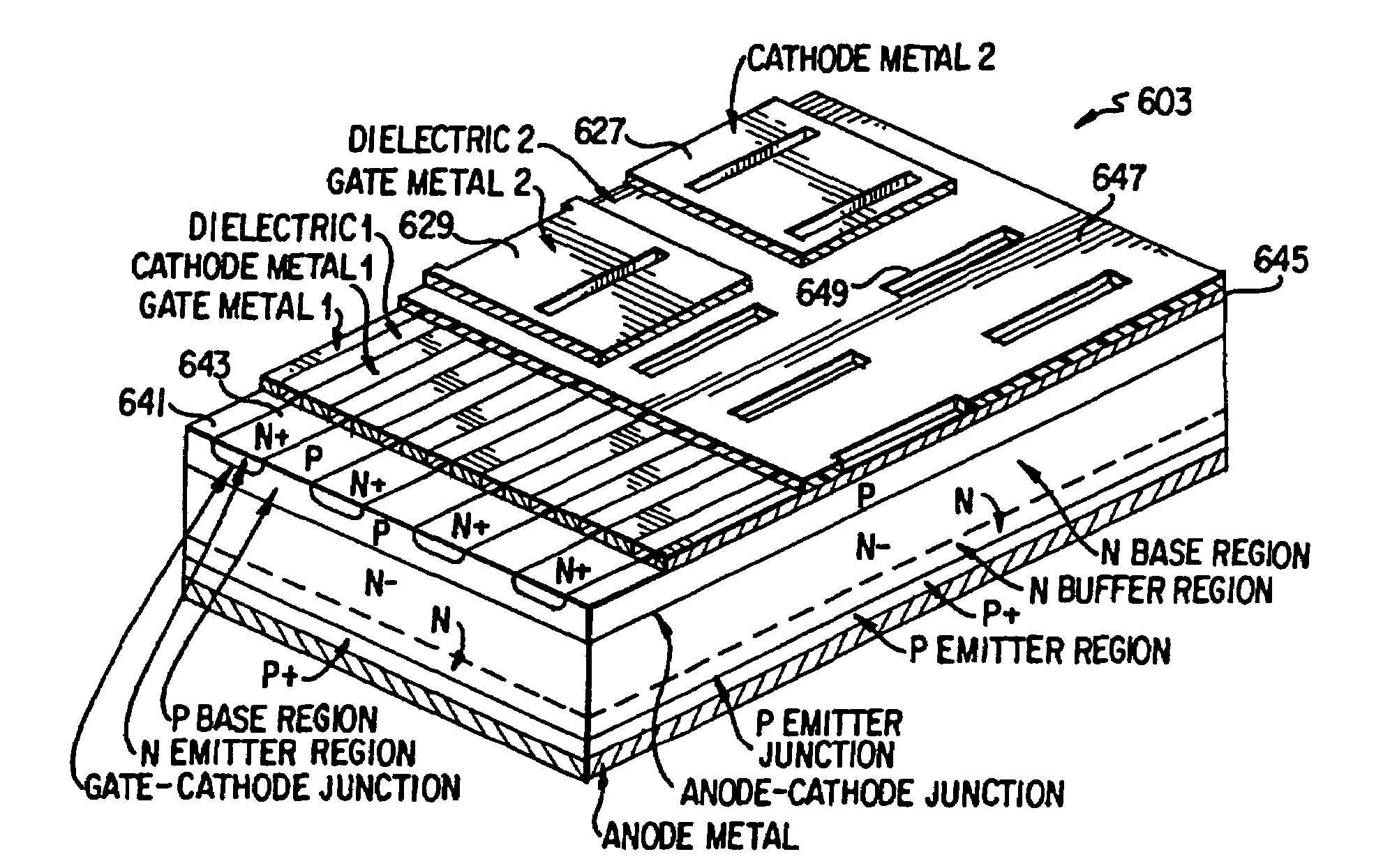
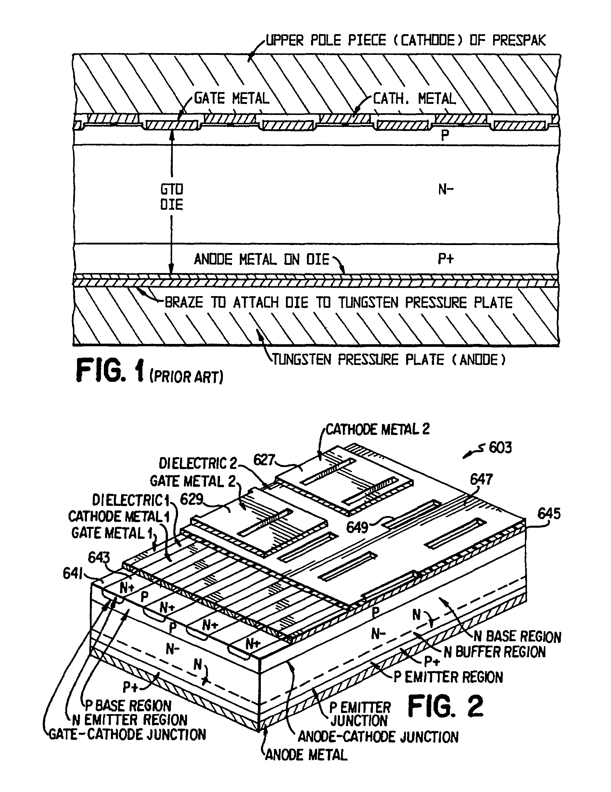
[0040]Turning next to FIG. 2, a first embodiment of the GTO die 603 is shown. The GTO 603 includes an anode metal layer, (P+) emitter region, (N) buffer region, (N−) base region, and a (P) base region 641 having (N+) emitter region channels 643 extending parallel to one another.

[0041]A differential inductance occurs between the (N+) region 643 and the (P) region 641. The present invention minimizes the differential induction to less than about 0.01 of the total inductance. A uniform current is provided, which depends upon finger width and resistance, to achieve a low total inductance and a uniform inductance. In addition, the (N+) emitter 643 has a repeating pattern along the cell of good and moderate injection regions of turn off capability. This pattern minimizes over...


PUM


Abstract

A gate turn-off thyristor (GTO) device has a lower portion, an upper portion and a lid. The lower portion has a lower base region of a first conductivity type, and a lower emitter region of a second conductivity type disposed at or from a lower surface of the lower base region. A lower junction is formed between the lower base region and the lower emitter region. The upper portion has an upper base region of the second conductivity type, and upper emitter regions of the first conductivity type disposed at or from an upper surface of the upper base region. An upper-lower junction is formed between the lower base region and the upper base region, and upper junctions are formed between the upper base region and the upper emitter regions. The upper base region and upper emitter regions form an upper base surface with first conductive contacts to the upper base region alternating with second conductive contacts to the upper emitter regions. The lid has a layer of insulator with upper and lower surfaces. Upper metal stripes extend along the upper surface of the insulator, and lower metal stripes extend along the lower surface of the insulator. The upper and lower metal stripes are connected together by vias that extend through the insulator. One set of the lower metal stripes contacts the first conductive contacts, but not the second conductive contacts. Another set of the lower metal stripes contacts the second conductive contacts, but not the first conductive contacts.

Description

[0001]The present invention claims the benefit of U.S. Provisional Application No. 60 / 302,386 filed Jul. 3, 2001, whose disclosure is hereby incorporated by reference in its entirety.BACKGROUND OF THE INVENTION[0002]1. Field of the Invention[0003]The invention relates to a gate turn-off thyristor having uniform current, low impedance and ultra-low gate impedance differential to all parts of the device.[0004]2. Description of the Related Art[0005]Conventional Gate Turn-off thyristors (GTO) are made with large feature sizes and emitters that are defined by deep silicon etches. Those GTOs are designed to accommodate large gate currents that flow in the gate metalization in turn-off and so that the gates are not shorted to the cathode when packaged in the standard hockey puck (or PressPak) package. Advanced GTOs having fine linewidths can be made in modern wafer fabrication facilities. However, providing low inductance and resistance gate contacts to all parts of the devices has not bee...

Claims


Application Information

Patent Timeline
Patent Type & Authority Patents(United States)
IPC IPC(8): H01L29/74H01L23/48H01L29/08H01L29/744
CPCH01L24/72H01L29/0834H01L29/744H01L2924/1305H01L2924/1301H01L2924/10253H01L2924/01033H01L2924/01006H01L2924/01013H01L2924/01015H01L2924/01029H01L2924/01042H01L2924/01074H01L2924/01075H01L2924/13055H01L2924/13091H01L2924/19043H01L2924/30107H01L2924/3011H01L2924/01005H01L2924/00
Inventor TEMPLE, VICHOLROYD, FORRESTAL-MARAYATI, SABIHPATTANAYAK, DEVA
Owner EXCELITAS TECH
Why Eureka
Try Eureka