Manufacturing method of semiconductor device

a manufacturing method and semiconductor technology, applied in the direction of semiconductor devices, electrical equipment, basic electric elements, etc., can solve the problems of source/drain increase and inability to achieve high-speed operation, and achieve the effect of improving the performance of the semiconductor devi

Inactive Publication Date: 2010-04-20
RENESAS ELECTRONICS CORP
View PDF21 Cites 6 Cited by
  • Summary
  • Abstract
  • Description
  • Claims
  • Application Information

AI Technical Summary

Benefits of technology

[0011]As for the metal silicide layer formed in the front surface of the electric conduction film which forms a gate, and the semiconductor region which forms a source / drain according to a salicide process, consisting of nickel silicide is more preferred than cobalt silicide from the request of the resistance reduction by microfabrication. By making a metal silicide layer into the nickel silicide instead of cobalt silicide, resistance of a metal silicide layer can be made lower and the diffusion resistance of a source / drain, contact resistance, etc. can be reduced more. Since a metal silicide layer can be formed thinly and the junction depth of a source / drain can be made shallow by making a metal silicide layer into the nickel silicide instead of cobalt silicide, it becomes advantageous to the microfabrication of a field-effect transistor.
[0013]In cobalt silicide formation, Si (silicon) is a diffusion seed, and cobalt silicide is formed when Si moves in Co film. On the other hand, in nickel silicide formation, Ni (nickel) is a diffusion seed, and nickel silicide is formed when Ni (nickel) moves to the silicon region side. For this reason, unnecessary NiSi2 portion is formed by Ni (nickel) diffusing superfluously in a salicide process, and the electric resistance of a metal silicide layer may vary for every field-effect transistor. For the further improvement in performance of a field-effect transistor, to reduce the variation in the electric resistance of the metal silicide layer for every field-effect transistor, and to prevent change of the characteristics of a field-effect transistor is desired.
[0014]A field-effect transistor is formed in the active region specified (surrounded) by the element isolation formed in the main surface of a semiconductor substrate. When element isolation is formed by the LOCOS method, element isolation does not give compressive stress to an active region. However, when element isolation is formed by the STI method, the compressive stress that the side wall of the trench for element isolation formed in the semiconductor substrate pushes the active region side acts. Therefore, it will be in the state where compressive stress is working to the active region of the semiconductor substrate by element isolation. A field-effect transistor tends to be formed in the active region where the compressive stress by element isolation has generated, and a NiSi layer is going to be formed in a salicide process on the semiconductor region which forms the source / drain. Then, analyses of the present inventor showed compressive stress promoting the anomalous diffusion of Ni and becoming easy to generate the abnormal growth of NiSi2 from a NiSi layer to a channel section. The abnormal growth of NiSi2 from this NiSi layer to a channel section is the problem that does not generate when element isolation is formed by the LOCOS method, but is first generated when making compressive stress act on the active region around which element isolation is formed by the STI method. When NiSi2 is doing abnormal growth to the channel section from the NiSi layer, increase of the leakage current between the source / drains of a field-effect transistor will be caused, or increase of the diffusion resistance of a source / drain region will be caused. Therefore, for the further improvement in performance of a field-effect transistor, to prevent such abnormal growth of NiSi2 from a NiSi layer to a channel section is desired.
[0015]The purpose of the present invention is to offer the technology which can improve the performance of a semiconductor device.

Problems solved by technology

However, resistance of a gate or a source / drain increases and the problem that high-speed operation is not obtained even if microfabrication of the field-effect transistor is done happens.

Method used


Image

  • Manufacturing method of semiconductor device
  • Manufacturing method of semiconductor device
  • Manufacturing method of semiconductor device

Examples


embodiment 1

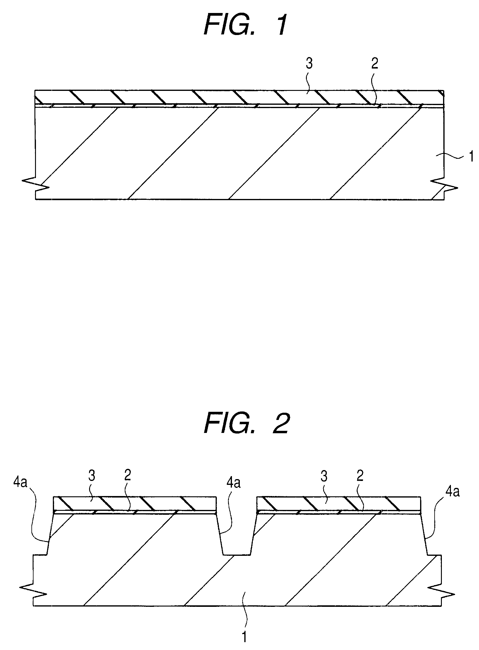
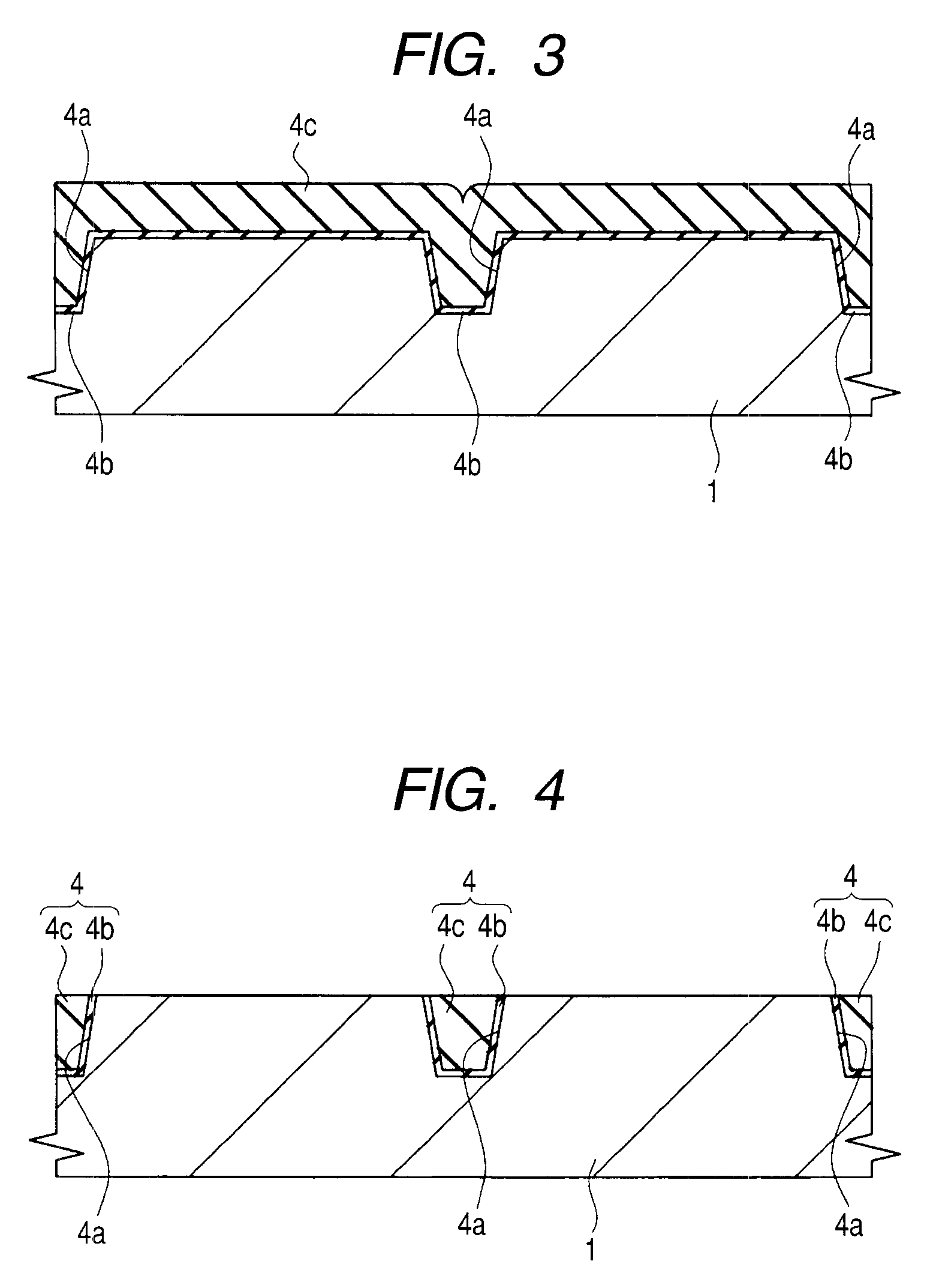
[0059]The manufacturing process of the semiconductor device of this embodiment is explained with reference to drawings. FIG. 1-FIG. 8 are the principal part cross-sectional views in the manufacturing process of the semiconductor device which is the 1 embodiment of the present invention. For example, they are principal part cross-sectional views in the manufacturing process of the semiconductor device which has CMISFET (Complementary Metal Insulator Semiconductor Field Effect Transistor).

[0060]First, as shown in FIG. 1, semiconductor substrate (semiconductor wafer) 1 which consists of p type single crystal silicon which has the specific resistance of about 1˜10Ω cm is prepared. Next, this semiconductor substrate 1 is oxidized thermally and insulation film 2 of about 10 nm thick is formed in the front surface. Then, insulation film 3 of about 100 nm thick is deposited on the upper layer by the CVD (Chemical Vapor Deposition) method etc., for example. Insulation film 2 consists of sili...

embodiment 2

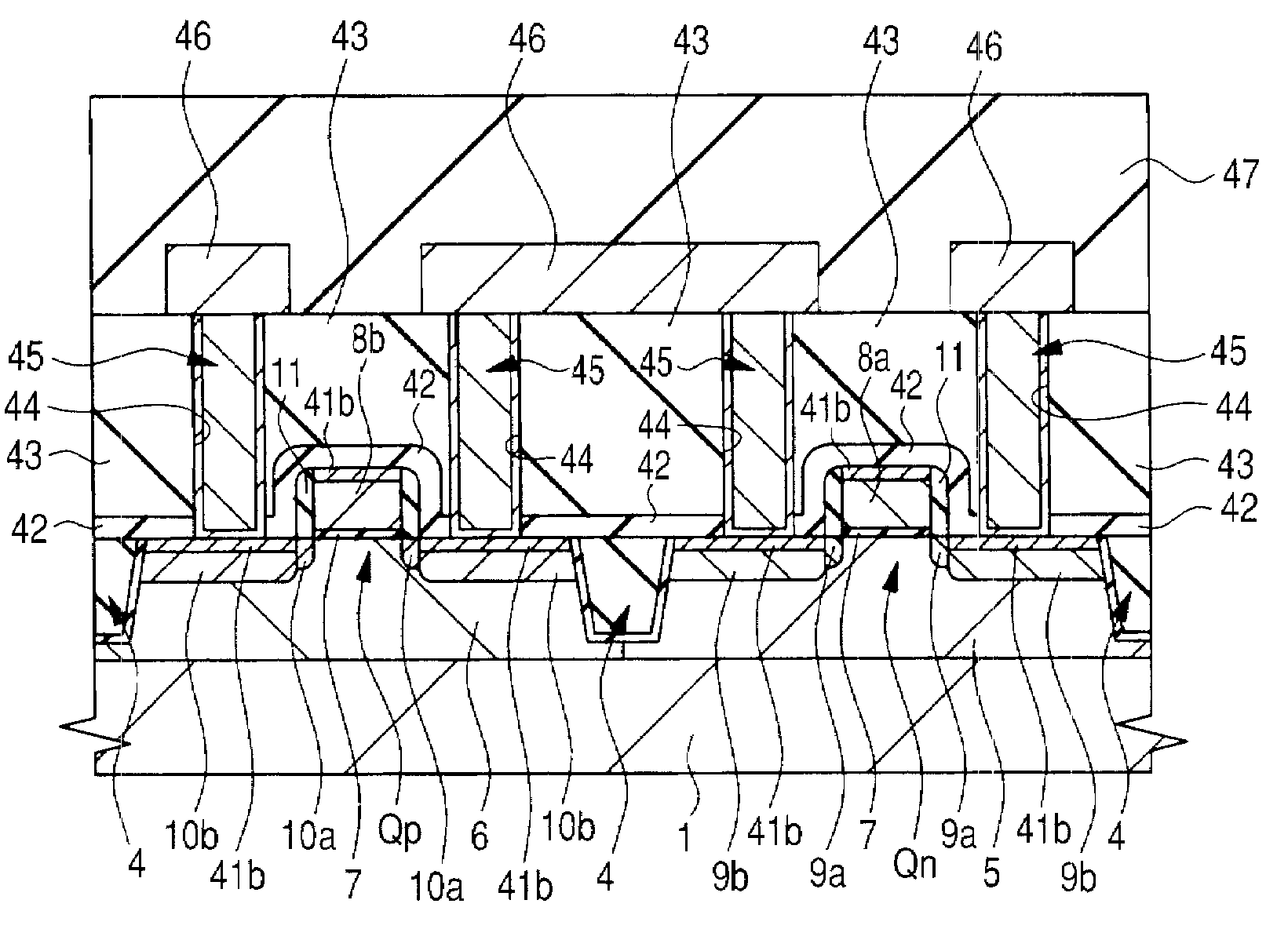
[0164]FIG. 25 is a manufacture process-flow chart showing a part of manufacturing process of the semiconductor device of this embodiment, and corresponds to the FIG. 9 of above-mentioned Embodiment 1. After the structure of the above-mentioned FIG. 7 is acquired, the manufacture process flow of the step which forms a metal silicide layer (metal and semiconductor reaction layer) in the front surface of gate electrodes 8a and 8b, n+ type semiconductor region 9b, and p+ type semiconductor region 10b according to a salicide process is shown in FIG. 25. FIG. 26-FIG. 29 are the principal part cross-sectional views in the manufacturing process of the semiconductor device of this embodiment.

[0165]Until the step which removes barrier film 13 and unreacted metallic film 12 by performing a wet cleaning treatment at the above-mentioned step S4, the step of the manufacturing process of the semiconductor device of this embodiment is the same as that of above-mentioned Embodiment 1. Therefore, the...

embodiment 3

[0179]FIG. 30 is a manufacture process-flow chart showing the manufacturing process of the semiconductor device of this embodiment, and corresponds to the FIG. 9 of above-mentioned Embodiment 1, or the FIG. 25 of above-mentioned Embodiment 2. The manufacture process flow of the step which forms a metal silicide layer (metal and semiconductor reaction layer) in the front surface of gate electrodes 8a and 8b, n+ type semiconductor region 9b, and p+ type semiconductor region 10b according to a salicide process after the structure of the above-mentioned FIG. 7 is acquired is shown in FIG. 30. FIG. 31-FIG. 34 are the principal part cross-sectional views in the manufacturing process of the semiconductor device of this embodiment.

[0180]Until the step which forms barrier film 13 at the above-mentioned step S2, the step of the manufacturing process of the semiconductor device of this embodiment is the same as that of above-mentioned Embodiment 1. Therefore, the explanation is omitted here an...


PUM

PropertyMeasurementUnit
temperatureaaaaaaaaaa
thicknessaaaaaaaaaa

Abstract

The performance of the semiconductor device which formed the metal silicide layer in the salicide process is improved. An element isolation region is formed in a semiconductor substrate by the STI method, a gate insulating film is formed, a gate electrode is formed, n+ type semiconductor region and p+ type semiconductor region for source / drains are formed, a metallic film is formed on a semiconductor substrate, and a barrier film is formed on a metallic film. And after forming the metal silicide layer to which a metallic film, and a gate electrode, n+ type semiconductor region and p+ type semiconductor region are made to react by performing first heat treatment, a barrier film, and an unreacted metallic film are removed, and the metal silicide layer is left. An element isolation region makes compressive stress act on a semiconductor substrate. A barrier film is a film which makes a semiconductor substrate generate tensile stress, and the metal silicide layer which consists of mono-silicide MSi of metallic element M which forms a metallic film is formed in the first heat treatment.

Description

CROSS-REFERENCE TO RELATED APPLICATION[0001]The present application claims priority from Japanese patent application No. 2007-81147 filed on Mar. 27, 2007, the content of which is hereby incorporated by reference into this application.FIELD OF THE INVENTION[0002]The present invention relates to a manufacturing method of a semiconductor device, and particularly relates to an effective technology in the application to manufacture of the semiconductor element which has a metal silicide layer.DESCRIPTION OF THE BACKGROUND ART[0003]According to a scaling rule, microfabrication of the field-effect transistor (MISFET:Metal Insulator Semiconductor Field Effect Transistor) is done as high integration of a semiconductor device progresses. However, resistance of a gate or a source / drain increases and the problem that high-speed operation is not obtained even if microfabrication of the field-effect transistor is done happens. Then, the salicide technology which reduces resistance of a gate and ...

Claims


Application Information

Patent Timeline
Patent Type & Authority Patents(United States)
IPC IPC(8): H01L21/00
CPCH01L21/823807H01L29/7846H01L29/665H01L29/7843H01L21/823835H01L21/823814
Inventor FUTASE, TAKUYAKASHIHARA, KEIICHIROOKADA, SHIGENARI
Owner RENESAS ELECTRONICS CORP
Why Eureka
Try Eureka