Liquid crystal panel and driver device thereof

a technology of driver device and liquid crystal panel, which is applied in the direction of static indicating device, non-linear optics, instruments, etc., can solve the problems of low transparency, heavy and expensive finished product, and limited resistance touch panel siz

Active Publication Date: 2010-04-20
HANNSTAR DISPLAY CORPORATION
View PDF4 Cites 34 Cited by
  • Summary
  • Abstract
  • Description
  • Claims
  • Application Information

AI Technical Summary

Problems solved by technology

Resistive touch panels are usually limited to small size.
The separately manufactured liquid crystal display panel and touch panel result in a heavy and expensive finished product with low transparency.
There is an error between the measurements.

Method used


Image

  • Liquid crystal panel and driver device thereof
  • Liquid crystal panel and driver device thereof
  • Liquid crystal panel and driver device thereof

Examples


Embodiment Construction

[0020]The following description is of the best-contemplated mode of carrying out the invention. This description is made for the purpose of illustrating the general principles of the invention and should not be taken in a limiting sense. The scope of the invention is best determined by reference to the appended claims.

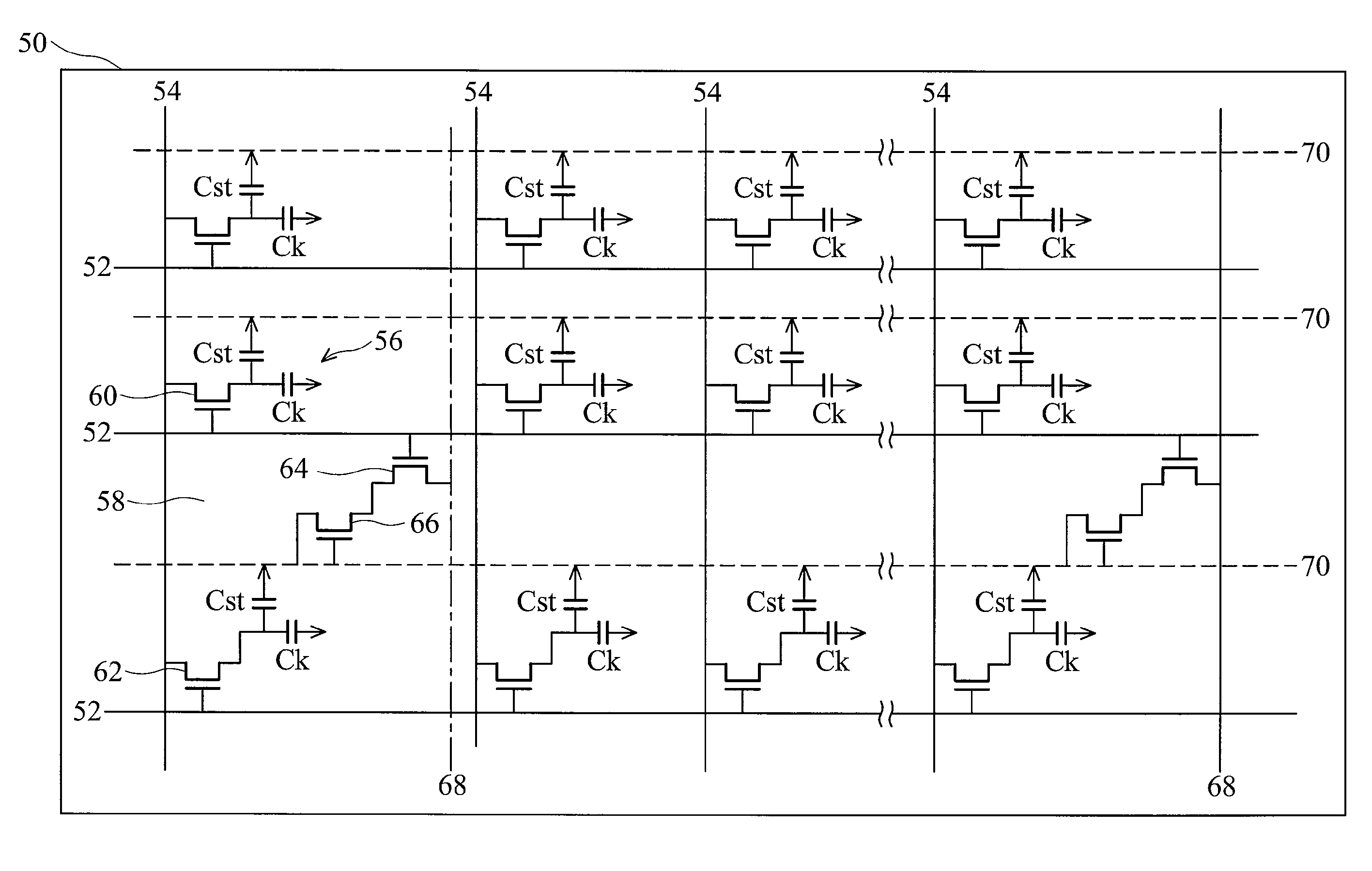
[0021]FIG. 3 illustrates an exemplary embodiment of the invention, a liquid crystal touch panel. As shown, a liquid crystal display panel comprises a plurality of scan lines 52 fabricated along a first axis, a plurality of data lines 54 fabricated along a second axis, a plurality of first pixels 56, and a plurality of second pixels 58. As shown in FIG. 3, each of the first pixels 56 is surrounded by two adjacent scan lines 52 and two adjacent data lines 54. The first pixel 56 comprises a first thin film transistor 60 having a gate electrically connected to one of the two adjacent scan lines, a source electrically connected to one of the data lines, and a drain electric...


PUM

PropertyMeasurementUnit
bias voltageaaaaaaaaaa
constant voltageaaaaaaaaaa
on-resistanceaaaaaaaaaa

Abstract

The invention provides a liquid crystal display panel, comprising a plurality of scan lines fabricated along a first axis, a plurality of data lines fabricated along a second axis, a first pixel and a second pixel. Each of the first and second pixels is surrounded by two adjacent scan lines and two adjacent data lines. The first pixel comprises a first thin film transistor (TFT). The second pixel comprises a second and a third TFT. The gates of the second and third TFT are electrically connected to the two adjacent scan lines surrounding the second pixel, respectively. The third TFT further comprises a source electrically connected to a photo-sensor, and a drain electrically connected to an access line fabricated along the second axis. One end of the access line is electrically connected to a signal processor via a switch.

Description

BACKGROUND OF THE INVENTION[0001]1. Field of the Invention[0002]The invention relates to liquid crystal panels, and particularly relates to the driver devices thereof.[0003]2. Description of the Related Art[0004]There are three types of touch panel: resistive, surface wave, and capacitive. Resistive touch panels are usually limited to small size. Surface wave touch panels register contact by electromagnetic response or by electromagnetic transmission. Capacitive touch panels register contact by capacitive response, with coordinates of the contact point evaluated according to variations in capacitance generated.[0005]Conventionally, touch panels and liquid crystal display panels are manufactured separately and combined into a finished product. The separately manufactured liquid crystal display panel and touch panel result in a heavy and expensive finished product with low transparency. To deal with the above drawbacks, a liquid crystal touch panel, which integrally fabricates the tou...

Claims


Application Information

Patent Timeline
Patent Type & Authority Patents(United States)
IPC IPC(8): G02F1/1343G09G3/36
CPCG02F1/13624G02F1/136286G02F2001/13312G02F1/13312
Inventor SHIH, PO-SHENGPAN, HSUAN-LIN
Owner HANNSTAR DISPLAY CORPORATION
Why Eureka
Try Eureka