Method for producing a conductor path on a substrate, and a component having a conductor path fabricated in accordance with such a method

a technology of conductor path and substrate, which is applied in the direction of non-metallic protective coating application, high frequency circuit adaptation, radiation controlled devices, etc., can solve the problems of unfavorable parasitic interference and electromagnetic loss, interference of neighboring conductor paths, and only minimal influence of conductor paths on component characteristics, etc., to achieve simple and cost-effective fabrication

Active Publication Date: 2010-04-27
ATMEL CORP
View PDF15 Cites 24 Cited by
  • Summary
  • Abstract
  • Description
  • Claims
  • Application Information

AI Technical Summary

Benefits of technology

[0010]It is therefore an object of the present invention to provide a method for producing a protected conductor path on a substrate and a component having a conductor path that was produced in accordance with such a method that ensures a simple and cost-effective fabrication of a conductor path that is protected and decoupled from the carrier substrate.
[0012]Compared to conventional technology, the present invention has the advantage that the conductor paths are freely suspended across the back-etched area of the substrate and a coupling between the conductor path and the substrate is avoided, or at least reduced. This results in low parasitic interferences. In addition, the membrane layer protects the conductor path due to an embedding feature of the invention, namely, embedding of the conductor path in the membrane. Thus, a component with at least one conductor path that is suspended from and protected by the membrane can be fabricated easier than a conventional component. This reduces both labor and production costs. Furthermore, the production method is compatible with silicon technologies for the high frequency field. Apart from the parasitic losses, the substrate losses in particular are substantially reduced. Compared to conventional production methods, the production method according to the present invention is, therefore, faster, simpler, and more cost-efficient and can also be realized by using a beneficial standard aluminum metallization.
[0013]In an example embodiment, an additional layer, particularly a first dielectric insulating layer, is formed on a top side of the substrate prior to the construction of the conductor paths. This additional layer can be beneficial in protecting the conductor path metallizations from possible etching agents.

Problems solved by technology

In general, undesirable parasitic interferences and electromagnetic losses occur due to interconnection contact of the conductor paths with the substrate.
In addition, interferences of neighboring conductor paths can occur due to the respective couplings of the conductor paths with the substrate.
At low frequencies, the influence of the conductor paths on the component characteristics is only minimal, however, at higher frequencies, particularly in the high frequency field, the electromagnetic effects of the conductor paths on the performance of the component can no longer be ignored.
However, the disadvantage of this approach proved to be the fact that such a production method is extremely complicated, time-consuming and costly.
Furthermore, another negative fact of this approach is that in addition to the fabrication of the membrane, a covering for the top-exposed conductor path must be provided to protect it from exterior influences.

Method used


Image

  • Method for producing a conductor path on a substrate, and a component having a conductor path fabricated in accordance with such a method
  • Method for producing a conductor path on a substrate, and a component having a conductor path fabricated in accordance with such a method
  • Method for producing a conductor path on a substrate, and a component having a conductor path fabricated in accordance with such a method

Examples


first embodiment

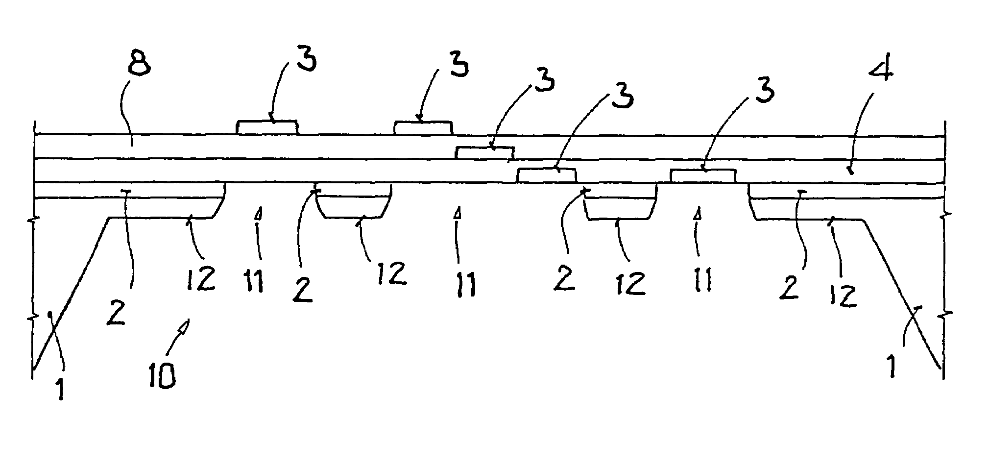
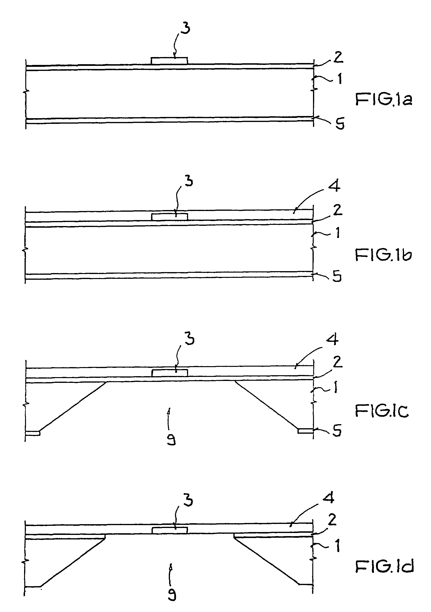
[0026]With reference to FIGS. 1a to 1d, a preferred embodiment for the construction of a metallic conductor path 3 on a substrate 1 is illustrated in detail. FIGS. 1a to 1d illustrate a sequence of the basic method steps in accordance with the present invention.

[0027]As shown in FIG. 1a, the starting point is a substrate 1. Preferably, the substrate 1 is a silicon semiconductor substrate, which can be relatively cost-efficiently fabricated, has a good thermal conductivity, and is suitable for integrated circuits in the high frequency field. The silicon substrate 1 can be a low-resistance or a high-resistance substrate, whereby high-resistance silicon substrates are more expensive.

[0028]To start with, for example, a first dielectric insulating layer 2 is formed, in a simple and conventional way, on the substrate 1, that is, on the top side of the substrate 1, which can, however, can be omitted in certain instances, and a further dielectric insulating layer 5 (henceforth referred to a...

second embodiment

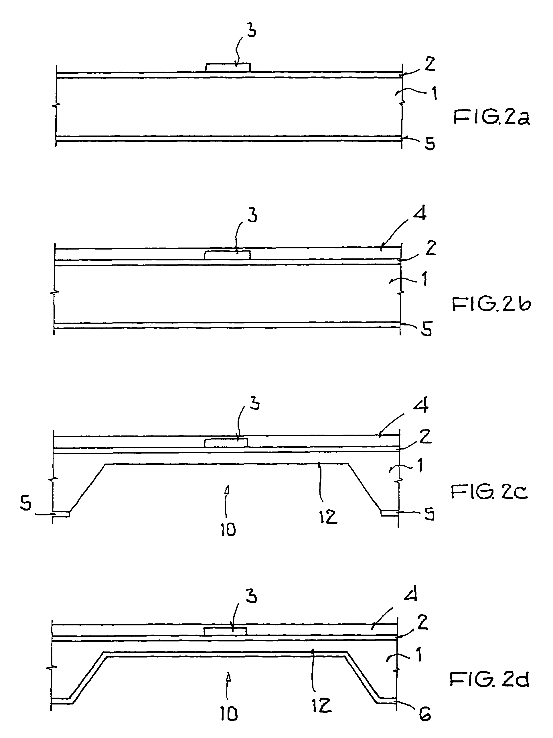
[0041]Referring to FIGS. 2a to 2g, a method of this invention for the construction of a metallic conductor path 3 on a substrate 1 is described in more detail below.

[0042]Since material selection, suitable etching steps or the like that were discussed in the first embodiment according to FIGS. 1a to 1d are equally applicable for the embodiment illustrated in FIGS. 2a to 2g, they will not be discussed in detail in the following section.

[0043]To start with, analogous to the previous embodiment and as illustrated in FIG. 2a, the substrate 1 is provided with a first dielectric insulating layer 2 on the top side of the substrate 1 and a further dielectric insulating layer 5 on the bottom side of the substrate 1, whereby under certain circumstances, these insulating layers can be omitted. Furthermore, the desired metallic conductor path 3 is also formed in a suitable location on the first dielectric insulation material 2, whereby it will be obvious to one skilled in the art that several c...


PUM


Abstract

A component having at least one conductor path on a substrate, and a production method for fabricating such a component is provided. The component is made by providing at least one conductor path on a predefined area of the substrate. Then a dielectric insulating layer is formed over the at least one conductor path, and a an area of the substrate is completely back etched below the at least one conductor path beginning on the bottom side of the substrate in such a way that the at least one conductor path is supported across the completely back-etched area of the substrate by adhesion to the second insulating layer.

Description

[0001]This nonprovisional application claims priority under 35 U.S.C. § 119(a) on German Patent Application No. DE 102004022178.2, which was filed in Germany on May 5, 2004, and which is herein incorporated by reference.BACKGROUND OF THE INVENTION[0002]1. Field of the Invention[0003]The present invention relates to a method for producing at least one conductor path on a substrate, and a component having at least one conductor path that is fabricated in accordance with such a method.[0004]Although it is applicable for any conductor path, the present invention describes in detail both the basic problems associated with it in regards to a conductor path for the electrical connection of two electronic components, for example, for two passive components, which are used in a high frequency field. This requires conductor paths on the substrate that are able to provide an interference-free transmission in the high frequency field.[0005]2. Description of the Background Art[0006]In general, u...

Claims


Application Information

Patent Timeline
Patent Type & Authority Patents(United States)
IPC IPC(8): H01L29/86H01L21/768H01L23/532H01L23/66H01L27/148H01P11/00H05K1/02H05K3/00H05K3/28
CPCH01L21/76838H01L23/66H01P11/003H05K1/024H01L2223/6627H01L2924/1903H01L2924/0002H05K3/0017H05K3/28H05K2201/0394H01L2924/00
Inventor JOODAKI, MOJTABA
Owner ATMEL CORP
Why Eureka
Try Eureka