Method for producing a conductor path on a substrate, and a component having a conductor path fabricated in accordance with such a method
a technology of conductor path and substrate, which is applied in the direction of non-metallic protective coating application, high frequency circuit adaptation, radiation controlled devices, etc., can solve the problems of unfavorable parasitic interference and electromagnetic loss, interference of neighboring conductor paths, and only minimal influence of conductor paths on component characteristics, etc., to achieve simple and cost-effective fabrication
- Summary
- Abstract
- Description
- Claims
- Application Information
AI Technical Summary
Benefits of technology
Problems solved by technology
Method used
Image
Examples
first embodiment
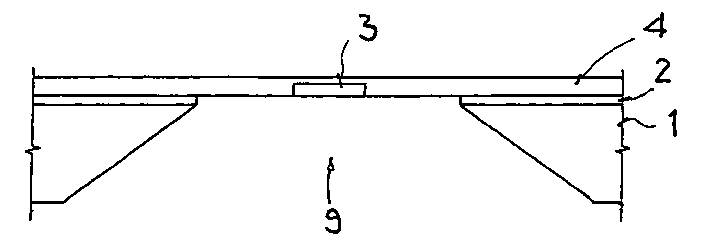
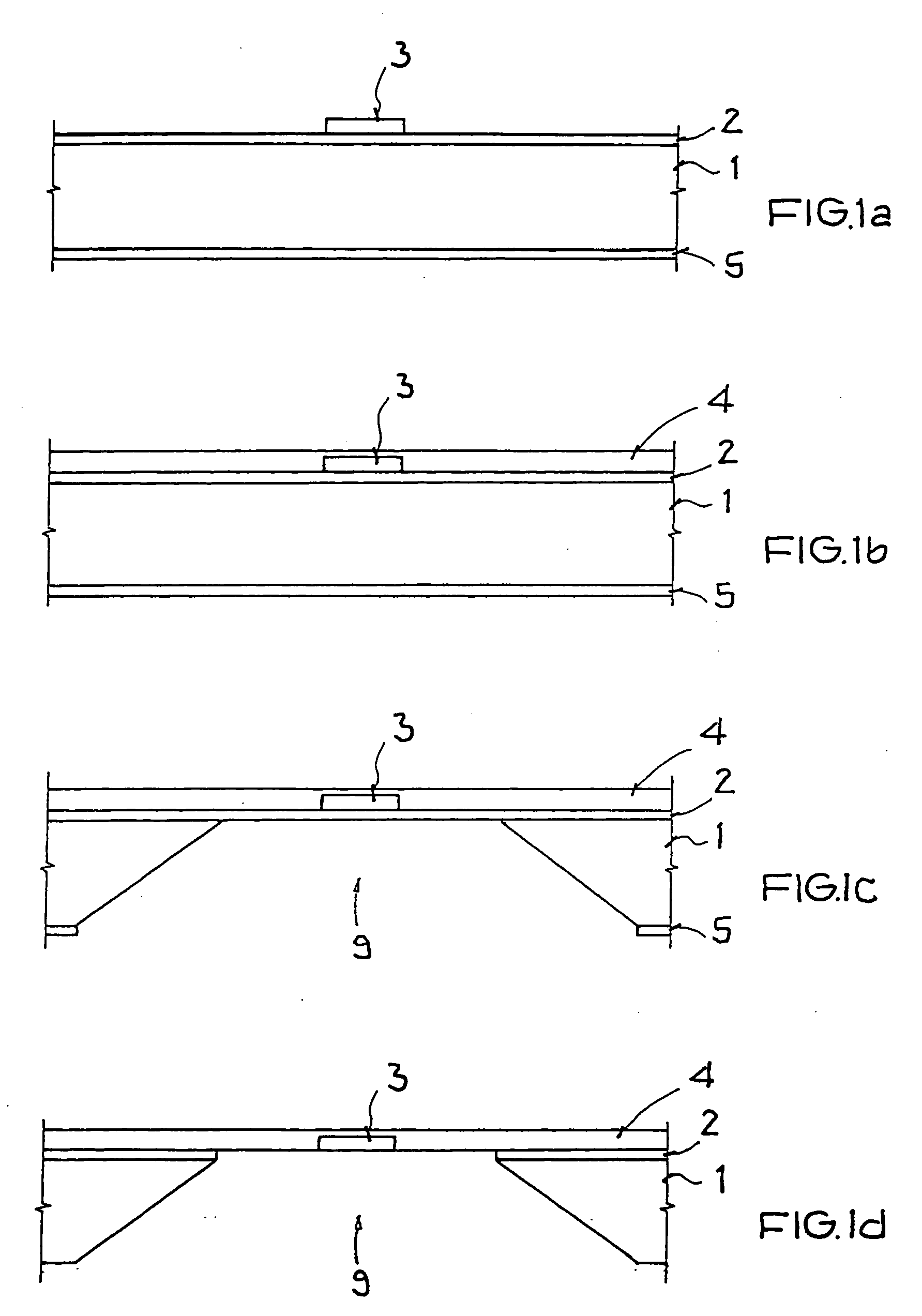
[0026] With reference to FIGS. 1a to 1d, a preferred embodiment for the construction of a metallic conductor path 3 on a substrate 1 is illustrated in detail. FIGS. 1a to 1d illustrate a sequence of the basic method steps in accordance with the present invention.
[0027] As shown in FIG. 1a, the starting point is a substrate 1. Preferably, the substrate 1 is a silicon semiconductor substrate, which can be relatively cost-efficiently fabricated, has a good thermal conductivity, and is suitable for integrated circuits in the high frequency field. The silicon substrate 1 can be a low-resistance or a high-resistance substrate, whereby high-resistance silicon substrates are more expensive.
[0028] To start with, for example, a first dielectric insulating layer 2 is formed, in a simple and conventional way, on the substrate 1, that is, on the top side of the substrate 1, which can, however, can be omitted in certain instances, and a further dielectric insulating layer 5 (henceforth referred ...
second embodiment
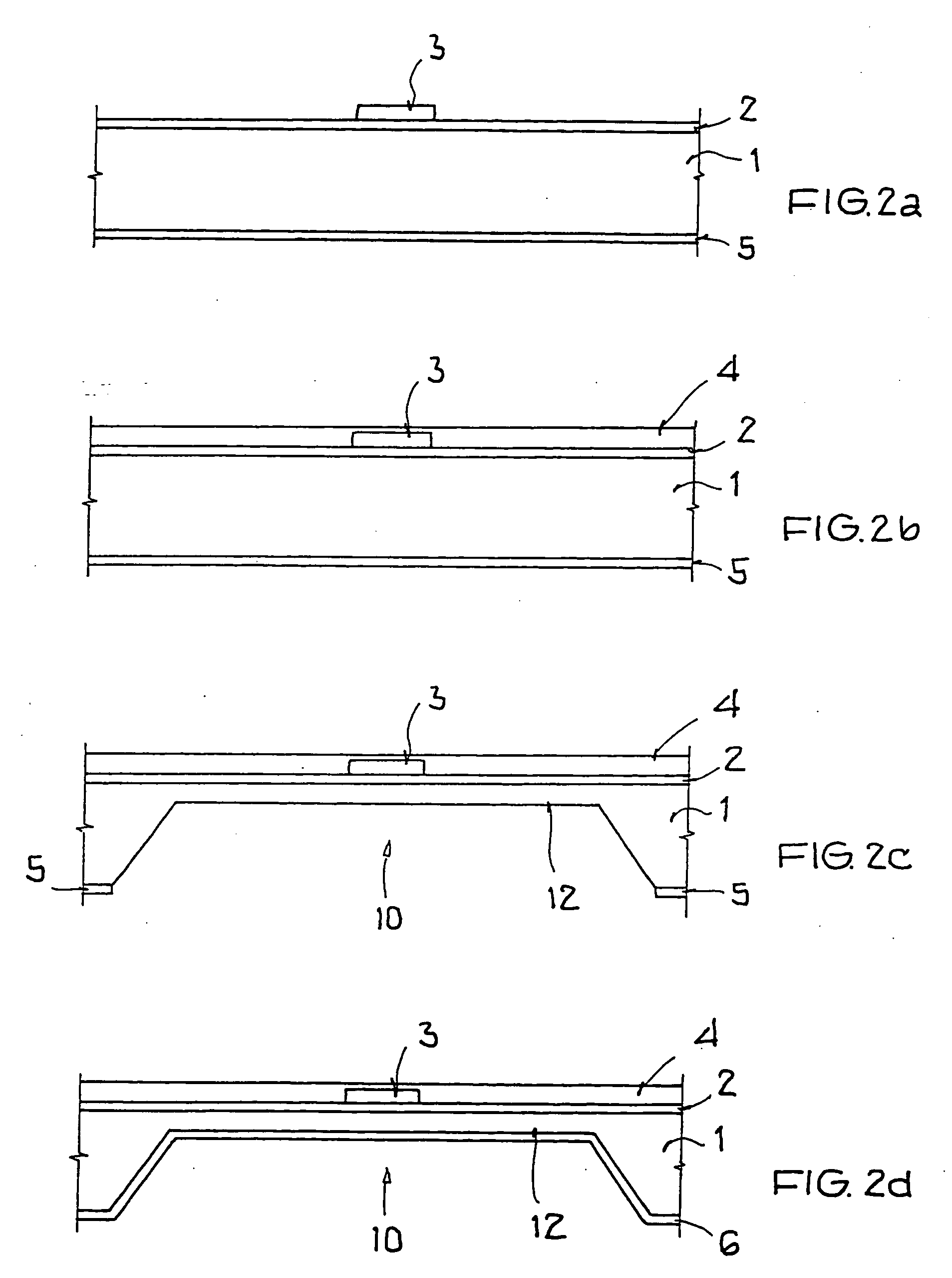
[0041] Referring to FIGS. 2a to 2g, a method of this invention for the construction of a metallic conductor path 3 on a substrate 1 is described in more detail below.
[0042] Since material selection, suitable etching steps or the like that were discussed in the first embodiment according to FIGS. 1a to 1d are equally applicable for the embodiment illustrated in FIGS. 2a to 2g, they will not be discussed in detail in the following section.
[0043] To start with, analogous to the previous embodiment and as illustrated in FIG. 2a, the substrate 1 is provided with a first dielectric insulating layer 2 on the top side of the substrate 1 and a further dielectric insulating layer 5 on the bottom side of the substrate 1, whereby under certain circumstances, these insulating layers can be omitted. Furthermore, the desired metallic conductor path 3 is also formed in a suitable location on the first dielectric insulation material 2, whereby it will be obvious to one skilled in the art that sever...
PUM
 Abstract
Description
Claims
Application Information


