Composite via structures and filters in multilayer printed circuit boards

a multi-layer printed circuit board and filter technology, applied in the direction of waveguides, waveguide type devices, high frequency circuit adaptations, etc., can solve the problems of radiation (leakage) loss and comparably large filter dimensions, and achieve the effect of high electrical performan

Inactive Publication Date: 2010-04-27
LENOVO INNOVATIONS LTD HONG KONG
View PDF2 Cites 29 Cited by
  • Summary
  • Abstract
  • Description
  • Claims
  • Application Information

AI Technical Summary

Benefits of technology

[0007]Three-dimensional arrangement of conductors in a filter developed by the use of composite via structures provides its compactness and the application of the ground vias provides its shielding and a high electrical performance.

Problems solved by technology

However, a planar structure of transmission line resonant stubs can lead to comparably large dimensions of filters as for an example at the frequency band up to 20 GHz.
Also radiation (leakage) losses can be considerable in such discontinuities as planar transmission line stubs.

Method used


Image

  • Composite via structures and filters in multilayer printed circuit boards
  • Composite via structures and filters in multilayer printed circuit boards
  • Composite via structures and filters in multilayer printed circuit boards

Examples


Embodiment Construction

[0024]The following description of the preferred embodiments directed to only several examples of composite via structures and filters provided by the use of some composite via structures but it is well understood that this description should not be viewed as narrowing the claims which follows.

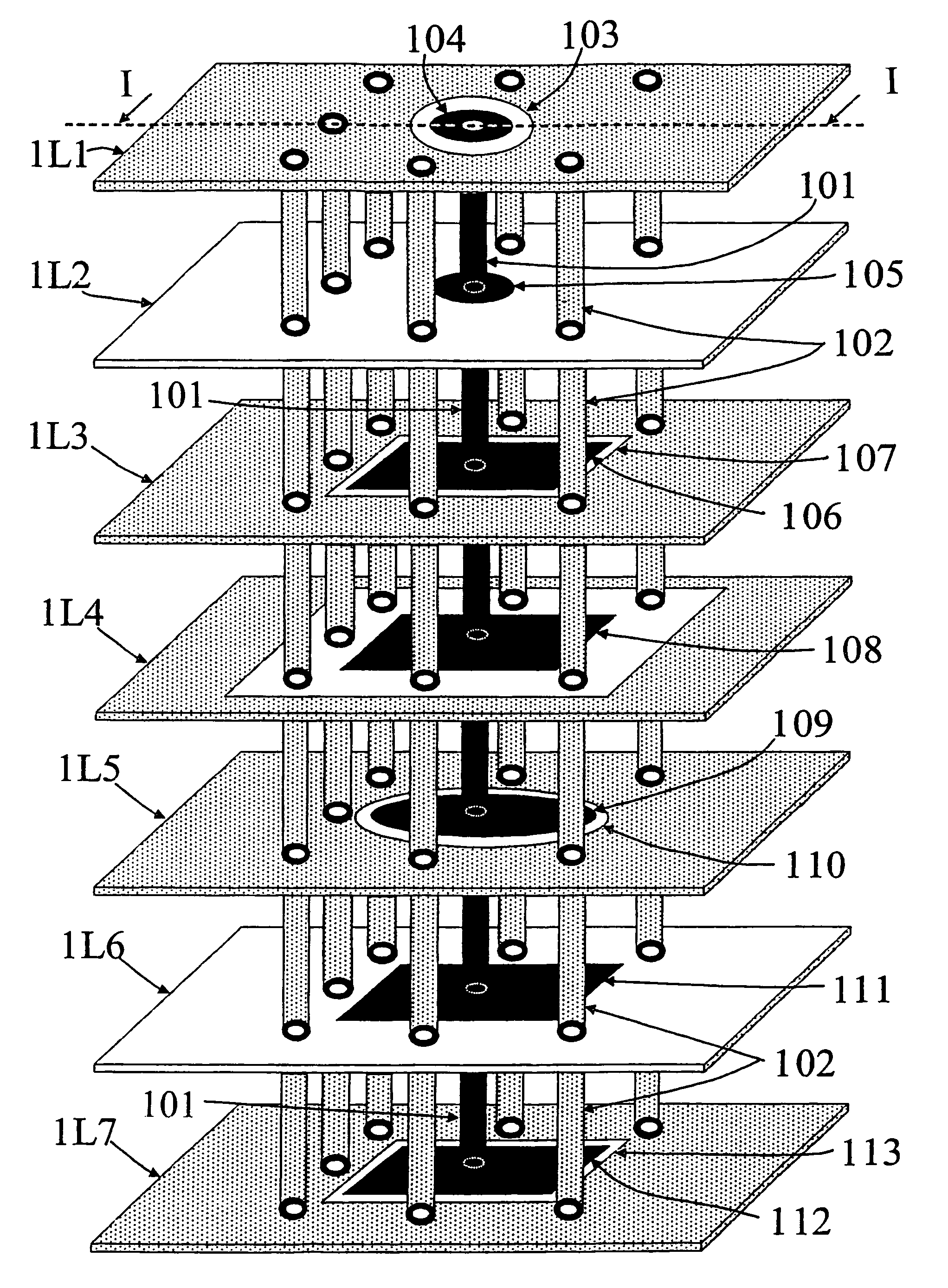
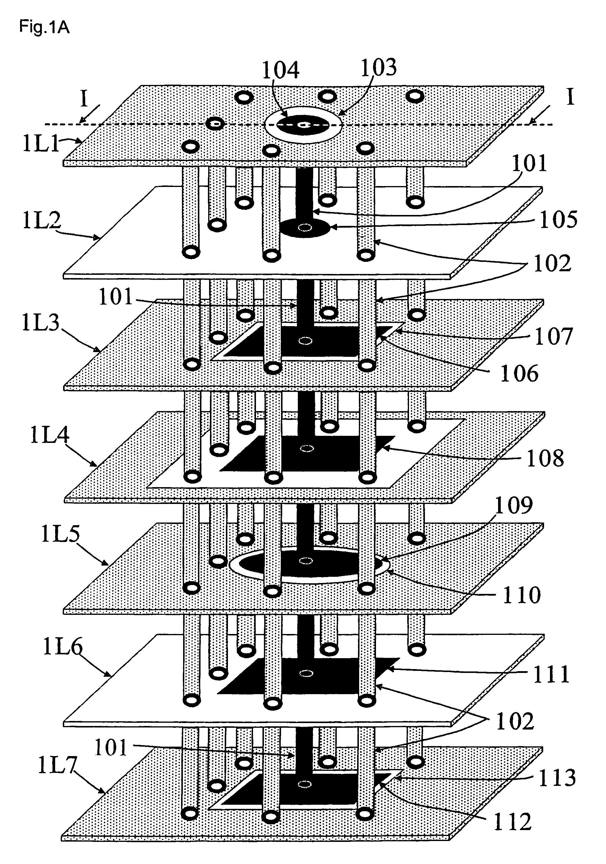
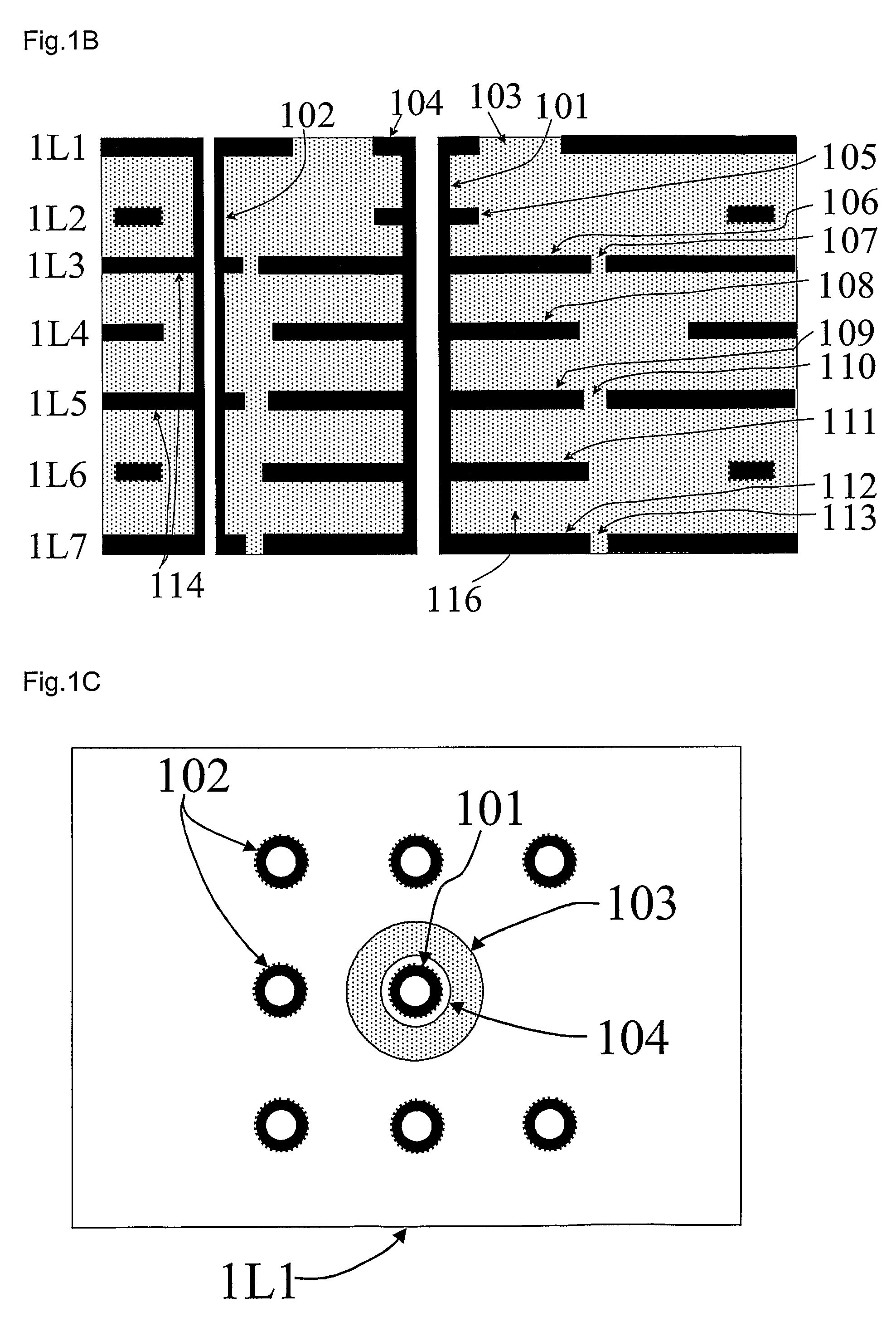
[0025]Referring to the drawings, a composite via structure in a 7-conductor-layer PCB, which serves only as an example of multilayer PCB design, is shown in FIGS. 1A, 1B, 1C and 1D. In these figures, the arrangement of conductor layers of the PCB separated by an isolating material 116 is as follows: Ground planes are 1L1, 1L3, 1L5 and 1L7 layers; Power supplying plane is 1L4 layer; and signal planes are 1L2 and 1L6 layers. The composite via structure unites two functional parts. First functional part provides a high-performance vertical transition from the first pad 104 to the special pad 105 disposed at the signal layer 1L2. Low return and leakage losses of this vertical transition including ...


PUM


Abstract

A composite via structure in a multilayer printed circuit board (PCB) and also compact and shielded filters formed by the use of composite via structures as building blocks are provided. The composite via structure consists of two functional parts. The first functional part is designed to form an interconnected circuit with low return and leakage losses between the first pad disposed at the one side of the PCB and the special pad serving for a connection to a planar transmission line. The second functional part of the composite via structure serves to form a shielded open- or short-circuited resonant length (stub) extended in the vertical direction from the special pad to the second pad disposed at the opposite side of the PCB.

Description

FIELD[0001]This invention relates generally to via structures and filters in multilayer printed circuit boards (PCBs). More specifically, the invention relates to composite via structures providing new compact filters including bandpass and bandstop ones in the multilayer PCB.BACKGROUND[0002]Usually a via structure in a multilayer printed circuit board (PCB) serves as a vertical transition between planar interconnected circuits based on planar transmission lines such as microstrip lines, striplines, coplanar lines and so on formed at different conductor layers of the PCB and are developed under the conditions providing low return and radiation (leakage) losses whole interconnect circuits used in electronic devices. These conditions stimulate the development different via structures such as blind vias, buried vias, shielded vias and so on.[0003]To develop components and devices based on PCB technologies, in particular filters, resonant lengths of the planar transmission lines such as...

Claims


Application Information

Patent Timeline
Patent Type & Authority Patents(United States)
IPC IPC(8): H01P1/20
CPCH01P1/2039H05K1/0222H05K1/0251H05K1/116H05K1/16H05K1/0237H05K2201/1006H05K2201/09618H05K2201/09627H05K2201/09718H05K2201/09781H05K2201/09809H05K3/429
Inventor KUSHTA, TARAS
Owner LENOVO INNOVATIONS LTD HONG KONG
Why Eureka
Try Eureka