Image display unit
a display unit and image technology, applied in static indicating devices, non-linear optics, instruments, etc., can solve the problems of slow response speed, lack of imaging repetition stability, difficult to maintain a stable dispersion state, etc., to achieve excellent stability, simple and inexpensive construction, and rapid response speed
- Summary
- Abstract
- Description
- Claims
- Application Information
AI Technical Summary
Benefits of technology
Problems solved by technology
Method used
Image
Examples
embodiment 1
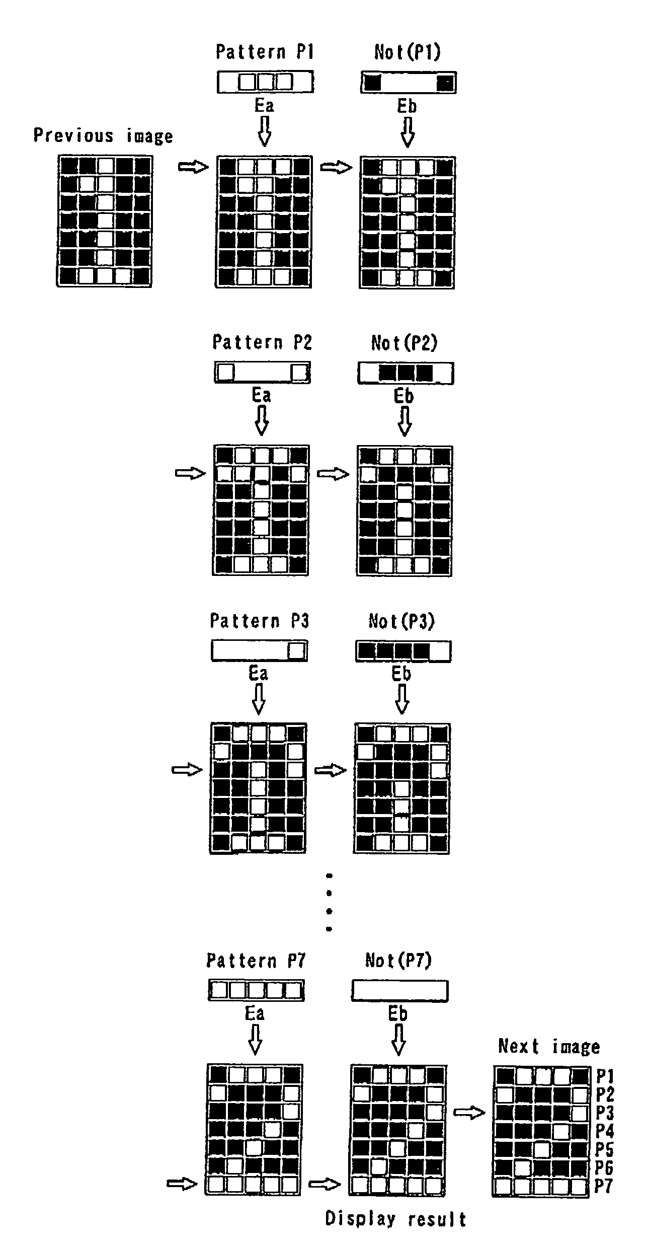
[0101]Hereinafter, a weiting means without using an image deleting process, which is a feature of the first aspect of the image display device according to the invention, will be explained with reference to drawings. In the examples shown in FIGS. 6 and 7, a rewriting operation from numeral “1” to numeral “2” is explained on the 7 lines×5 rows matrix display.
[0102]In the example shown in FIG. 6, the image is formed by switching a direction of the electric field to be applied sequentially during an image forming process of a portion where the display is rewritable at once (normally one line) on the 7 lines×5 rows matrix display. Specifically, if patterns of 1 . . . n lines of the image “2” to be written next are assumed as P1 . . . Pn, in order to switch the direction of the electric field at every one line, firstly the pattern P1 is written by Ea on the first line and then the pattern Not(P1) is written by Eb on the first line. Secondary, the pattern P2 is written by Ea on the secon...
embodiment 2
[0106]Then, the operation for the halftone image display (gray level display) and the particle sate reset operation prior to the halftone image display, which are performed by the second aspect of the image display device according to the invention, will be explained with reference to FIGS. 8a, 8b and FIG. 9.
[0107]FIG. 8a is a schematic view for explaining a method of applying a reset voltage for a particle state reset operation prior to a halftone image display in the image display device according to the second aspect of the invention, and FIG. 8b is a schematic view for explaining a method of applying an electric field for a halftone image display in the image display device according to the second aspect of the invention. In FIGS. 8a and 8b, a horizontally arranged rectangle corresponds to the display electrode 3, a vertically arranged rectangle corresponds to the opposed electrode 4, and an intersecting portion between the horizontally arranged rectangle and the vertically arra...
embodiment 3
[0114]FIGS. 10a to 10d are schematic views respectively showing one embodiment of sub-pixels in the third aspect of the image display device according to the invention. The embodiment shown in FIGS. 10a to 10d shows the sub-pixels obtained by segmentalizing one pixel unevenly. Specifically, one pixel (FIG. 10b) in the 20×20 dots matrix display shown in FIG. 10a is segmentalized into sub-pixels each having a different size. In this case, sizes of the sub-pixels are to be two's power i.e. six sub-pixels have sizes of 20(=1), 21(=2), 22(=4), 23(=8), 24(=16) and 25(=32) respectively.
[0115]As for a method of segmentalizing one pixel unevenly, as shown in FIG. 10c, use may be made of six sub-pixels each having a rectangular shape with a different area. Moreover, as shown in FIG. 10d, use may be made of six sub-pixels each having same width along a line direction and different width along a row direction, i.e. each having a different area. The uneven segmentalization shown in FIG. 10c is d...
PUM
| Property | Measurement | Unit |
|---|---|---|
| particle diameter | aaaaa | aaaaa |
| thickness | aaaaa | aaaaa |
| thickness | aaaaa | aaaaa |
Abstract
Description
Claims
Application Information


