Method for voltage limitation in a transponder

a transponder and circuit technology, applied in the direction of instruments, pulse techniques, burglar alarm mechanical actuation, etc., can solve the problems of undesirably high voltage, corrupt information transmission, and the destruction of the integrated circuit present in the tag

Active Publication Date: 2010-05-04
ATMEL CORP
View PDF15 Cites 4 Cited by
  • Summary
  • Abstract
  • Description
  • Claims
  • Application Information

AI Technical Summary

Benefits of technology

[0014]It is therefore an object of the present invention to provide a method and a circuit arrangement that eliminates the aforementioned disadvantage.
[0016]This method offers the advantage that for both voltage half-waves overall only one depletion layer component needs to be provided, whereas in prior-art methods a symmetric construction of at least one depletion layer component was provided per voltage half-wave.
[0027]It is especially advantageous here when a capacitor switchable by an inverse modulation signal is provided for driving the depletion layer component.

Problems solved by technology

At small distances between the reader and tag, depending on the transmitting power, such high voltages can be induced in the tag that an integrated circuit present in the tag can be destroyed.
As a result, the depletion layer elements act as a reliable limitation of the resonant circuit voltage to a corresponding value, even at high coil currents.
This is of particular importance in systems with high-quality inductors, which at close spatial proximity of the transmitting resonant circuit and the receiving resonant circuit could otherwise cause undesirably high voltages.
A problem has been observed with the load modulation from conventional circuits, which is, when during the activation of modulation, that is, when the resonant circuit voltage is limited to the lower clamping voltage, a high coil current is induced, the current drains typically through a bridging of Zener diodes and the remaining depletion layer elements that are switched in a forward direction, whereby the resonant circuit voltage can fall below the lower clamping voltage and even below a threshold value that is used for detecting oscillations (pulses) of the resonant circuit voltage.
With unfavorable phase conditions, therefore, it can happen that when the load is turned on, the voltage of the transmitting resonant circuit drops below a detection threshold for one or several periods due to feedback, which corrupts the information transmission.
This can cause data loss during information transmission to the reading device.

Method used


Image

  • Method for voltage limitation in a transponder
  • Method for voltage limitation in a transponder
  • Method for voltage limitation in a transponder

Examples


Embodiment Construction

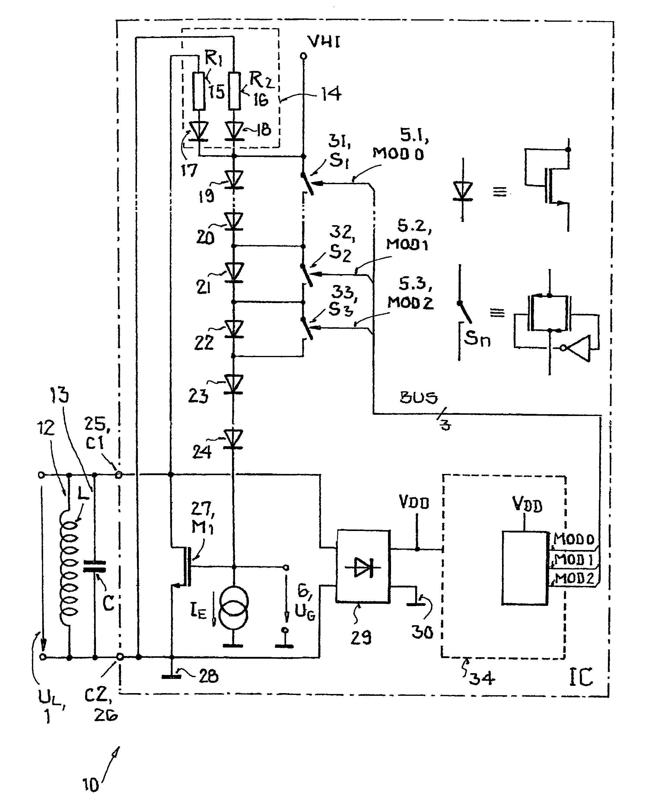
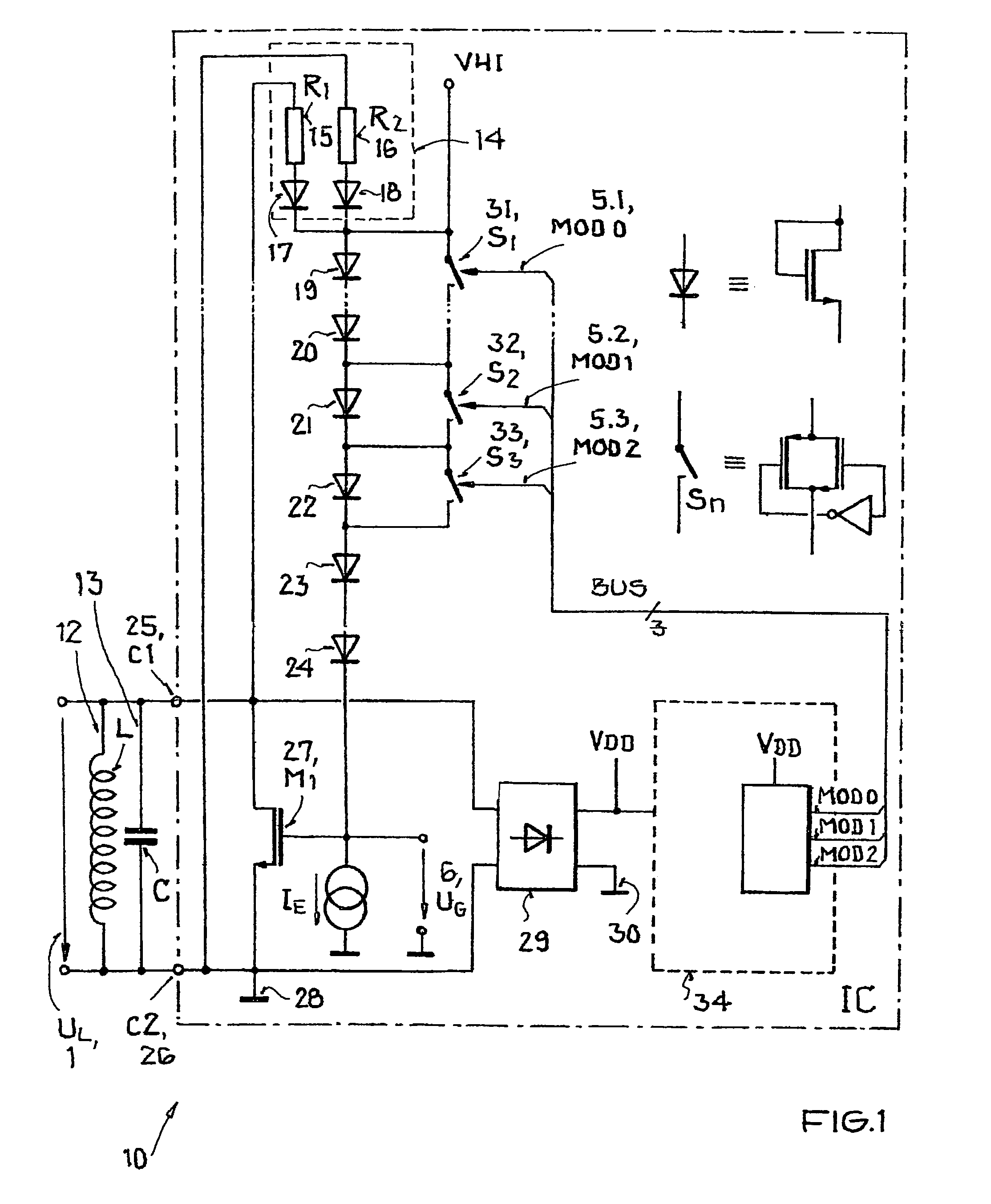
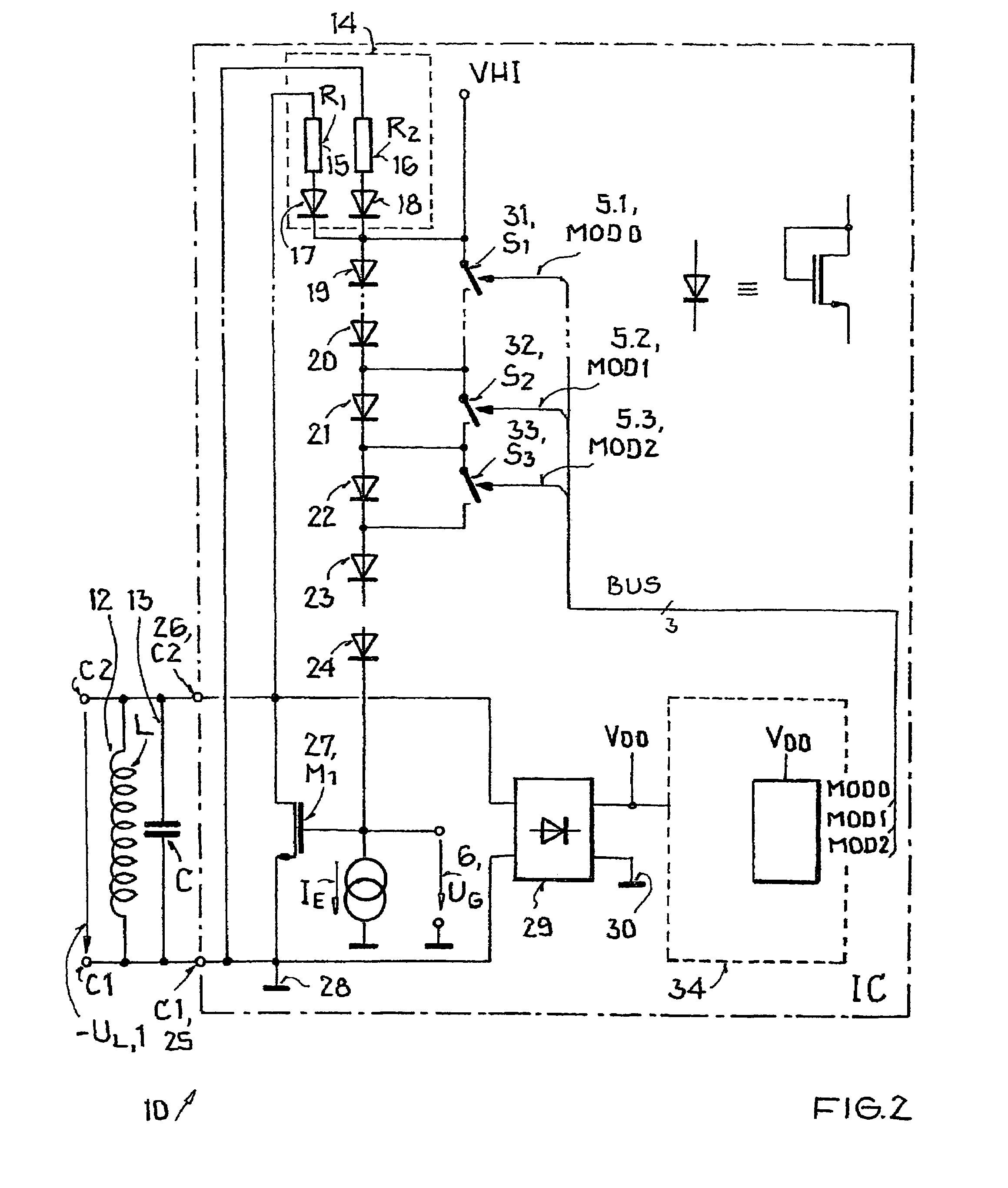
[0036]FIGS. 1 and 2 show a transmitting and receiving resonant circuit 10 of a receiving part or tag. Parallel to resonant circuit 10, which comprises an inductor L 12 and a capacitor C 13, a depletion layer component 27, such as an NMOS transistor is located between a first resonant circuit terminal C1 25 and a second resonant circuit terminal C2 26. At the output of depletion layer component 27, there is a reference potential terminal 28 which represents a ground potential for the circuit. Because depletion layer component 27 can switch between source and drain, the circuit in the present form can be used both for a first and for a second voltage half-wave.

[0037]Parallel to resonant circuit 10 and between the first C1 25 and second resonant circuit terminal C2 26, there is a series connection comprising polarity change circuit 14 and diodes 19, 20, 21, 22, 23, 24, which are used to drive depletion layer component 27. In this case, the diodes can be realized as NMOS transistors, wh...


PUM


Abstract

A circuit for voltage limitation is provided in a transponder with a resonant circuit, which comprises at least one inductor, a capacitor, a depletion layer component with an input, output, and a control input, a first resonant circuit terminal, which is connected to the input of the depletion layer element, and a second resonant circuit terminal, which is connected to the output of the depletion layer element, whereby there is a connection between the control input of the depletion layer component and the first resonant circuit terminal and the second resonant circuit terminal. A method for voltage limitation in a transponder is provided, whereby for voltage limitation in the transmitting and receiving resonant circuit, the control terminal of the depletion layer element is driven by the voltage of the first and second resonant circuit terminal.

Description

[0001]This nonprovisional application claims priority under 35 U.S.C. §119(a) on German Patent Application No. DE 102006006912, which was filed in Germany on Feb. 15, 2006, and which is herein incorporated by reference.BACKGROUND OF THE INVENTION[0002]1. Field of the Invention[0003]The present invention relates to a method for voltage limitation and to a circuit for voltage limitation in a transponder.[0004]2. Description of the Background Art[0005]Methods and circuits are known to one skilled in RFID (RFID=Radio frequency Identification). RFID is, for example, a transmitting resonant circuit that may supply an inductively coupled receiving resonant circuit with power and reads data via the receiving resonant circuit. Such connections are employed, for instance, for object identification, whereby a transmitting resonant circuit of a reading device (reader) responds to an object marked with a label (tag) via a receiving resonant circuit and retrieves information.[0006]To establish co...

Claims


Application Information

Patent Timeline
Patent Type & Authority Patents(United States)
IPC IPC(8): H02M1/32H02M1/34H03B1/00H03K7/00
CPCG06K19/0701H03G11/02G06K19/07749G06K19/0715
Inventor BERHORST, MARTINKURZ, ALEXANDERSCHNEIDER, PETER
Owner ATMEL CORP
Why Eureka
Try Eureka