
Semiconductor device

a technology of semiconductor devices and semiconductors, applied in the field of semiconductor devices, can solve the problems of inability to accurately measure the input setup and hold characteristics of devices under test, and the input signal contains a large error referred to as jitter,

Active Publication Date: 2010-05-04
MICRON TECH INC
View PDF6 Cites 2 Cited by
  • Summary
  • Abstract
  • Description
  • Claims
  • Application Information

AI Technical Summary

Benefits of technology

The present invention is a semiconductor device that improves the accuracy of measuring data at an input / output terminal by using a driver pin with less jitter. This is achieved by a circuit configuration that eliminates differences in jitter between the input / output terminal and the driver pin of the semiconductor test equipment or text board. The semiconductor device includes a signal selecting circuit and a latch circuit that work together to capture data and accurately measure the setup and hold characteristics of the semiconductor device. This results in more accurate data capture and improved performance of the semiconductor device.

Problems solved by technology

Further, since the slope of the waveform of the input signal supplied to the test board from the semiconductor test equipment is small, the input signal contains a large error referred to as jitter.
However, in Patent Documents 1 and 2, there is not disclosed any arrangement of reducing error in a measurement system for measuring the setup and hold characteristics of data, ascribable to the fact that the IO pin has a blunter waveform than the waveform of the driver pin.
As a result, a device under test (DUT) cannot capture a data signal received at an IO pin thereof responsive to a data strobe signal received at an IO pin thereof under accurate conditions.
A problem which arises, therefore, is that accurate input setup and hold characteristics cannot be measured.
In addition, since there will be a great amount of jitter, the output signal of the initial-stage circuit (receiver circuit) of the corresponding signal also will contain a large amount of jitter.

Method used


Image

  • Semiconductor device
  • Semiconductor device
  • Semiconductor device

Examples


Embodiment Construction

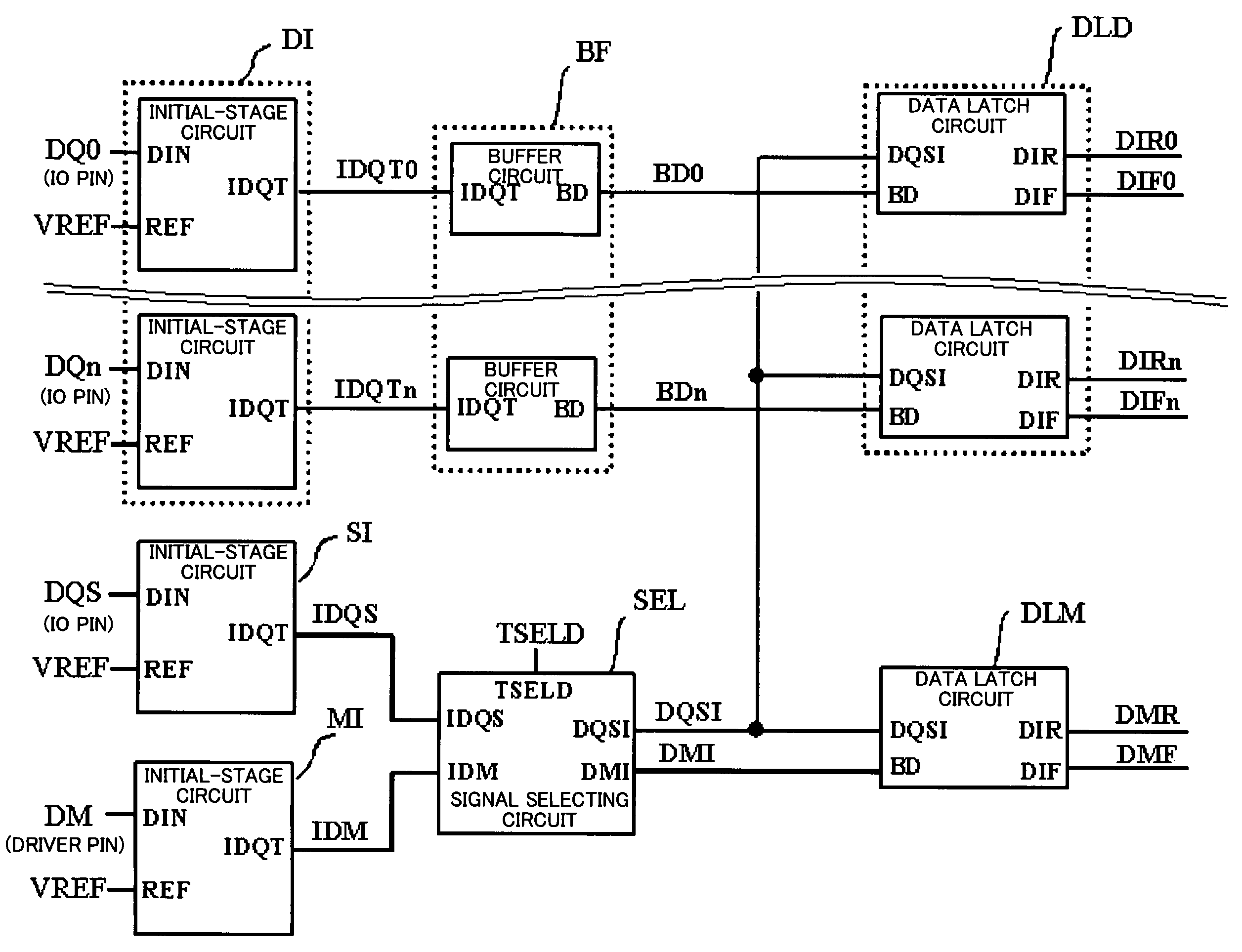
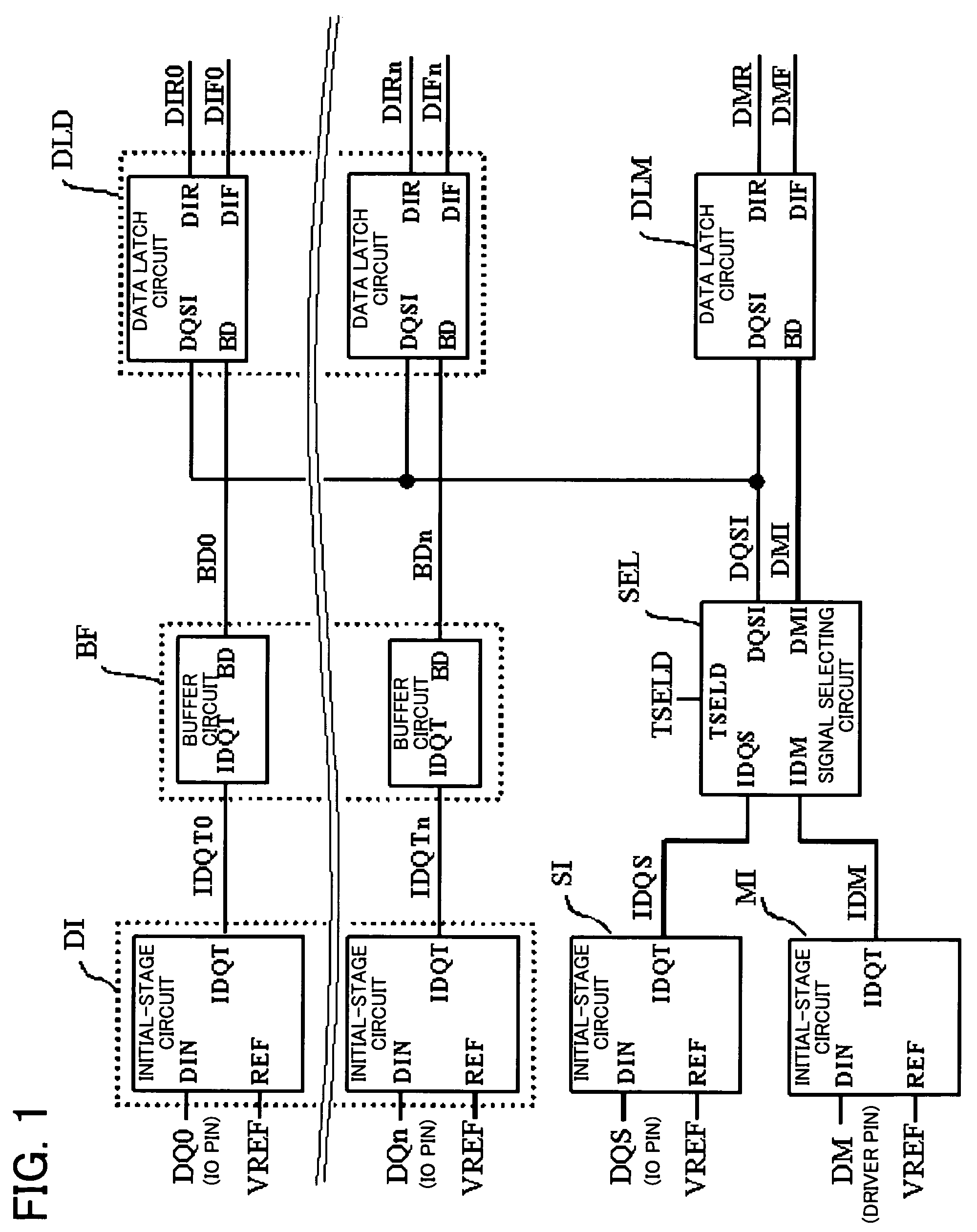
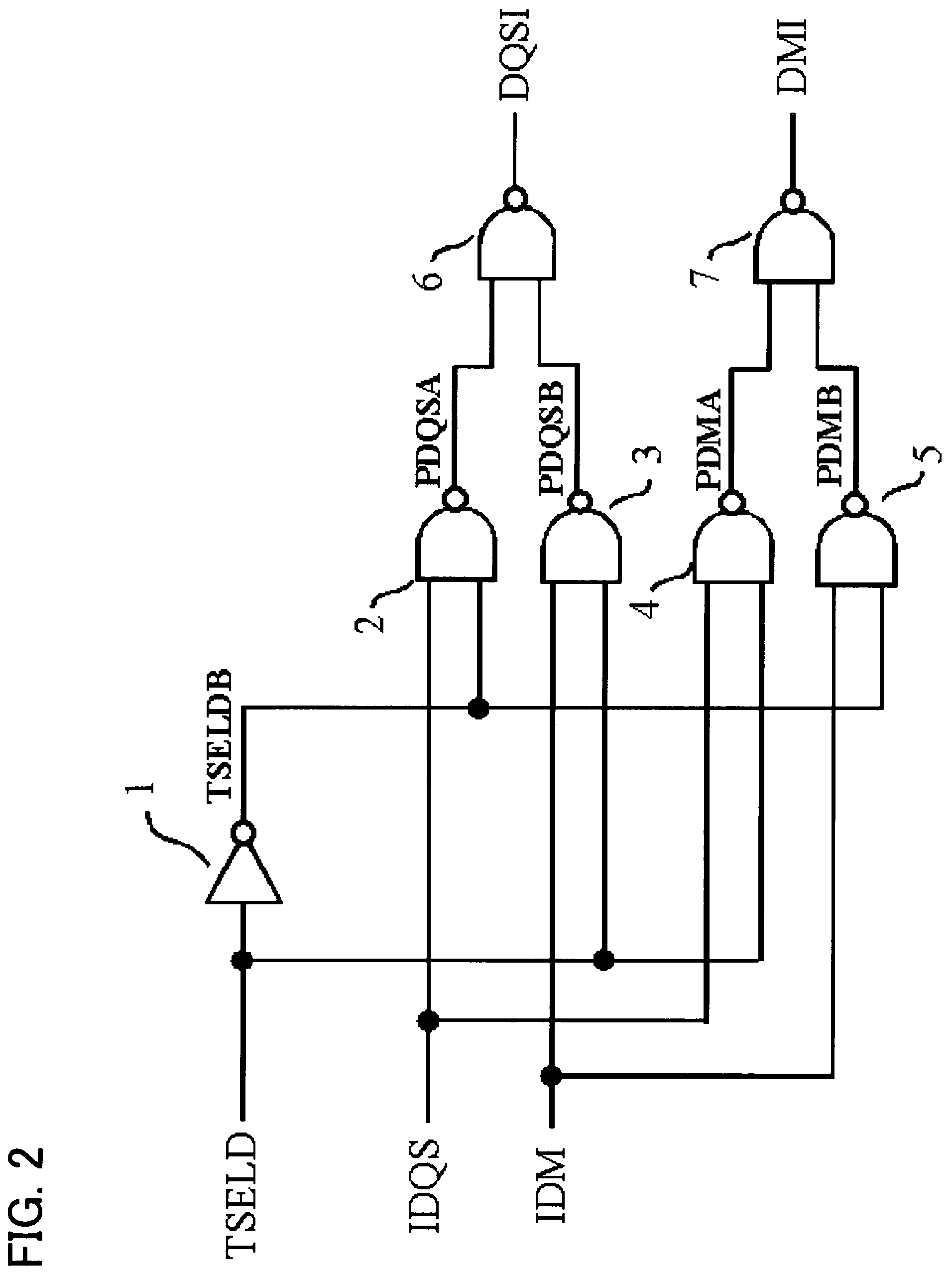
[0034]Preferred modes of the invention will be described with reference to the accompanying drawings. The present invention provides a semiconductor device having an input / output terminal for a strobe signal that decides input / output timing in data input / output, the device having a function whereby the output signal from an initial-stage circuit of an input / output terminal (the circuit receives supply of a signal from an IO pin of a semiconductor test equipment at the time of a test) and the output signal from an initial-stage circuit of a separate input terminal (the circuit receives supply of a signal from a driver pin of the semiconductor test equipment at the time of a test) can be interchanged in a mode setting or test function. By interchanging the signals, capturing of data from an IO pin of the semiconductor test equipment is performed by the small-jitter driver pin of the semiconductor test equipment. As a result, measurement of the setup and hold characteristics of inputs ...


PUM


Abstract

Disclosed is a semiconductor device comprising: a signal selecting circuit for receiving, at first and second inputs thereof, respectively, a first signal output from a first initial-stage circuit that receives a data strobe signal from a first terminal, which is an input / output terminal, and a second signal output from a second initial-stage circuit that receives a data mask signal from a second terminal, which is an input terminal, and based upon a control signal that is supplied thereto, outputting the first and second signals from first and second outputs or interchanging the first and second signals and outputting the interchanged first and second signals from the second and first outputs; a buffer circuit for receiving an output signal from a third initial-stage circuit that receives a data signal from a data terminal; and a data latch circuit for latching a signal from the buffer circuit. The signal from the first output of the signal selecting circuit is supplied to the data latch circuit as a latch timing signal.

Description

REFERENCE TO RELATED APPLICATION[0001]This application is based upon and claims the benefit of the priority of Japanese patent application No. 2007-146873, filed on Jun. 1, 2007, the disclosure of which is incorporated herein in its entirety by reference thereto.FIELD OF THE INVENTION[0002]This invention relates to a semiconductor device and, more particularly, to a semiconductor device having a configuration ideal for measuring AC characteristics such as setup and hold characteristics.BACKGROUND OF THE INVENTION[0003]In a semiconductor storage device that has an IO pin for receiving a strobe signal that decides input / output timing in data input / output, an output signal of an initial-stage circuit of the strobe signal at the IO pin, and an output signal of another initial-stage circuit of a driver pin which is separately provided from the IO pin, are interchanged in a mode setting or test function.[0004]FIG. 6 illustrates an example of a typical configuration of a semiconductor stor...

Claims


Application Information

Patent Timeline
Patent Type & Authority Patents(United States)
IPC IPC(8): G11C7/10
CPCG11C11/4096G11C29/56012G11C29/022G11C29/02
Inventor ARAI, MINARI
Owner MICRON TECH INC
Learn More