Semiconductor device

a technology of semiconductor devices and semiconductors, applied in semiconductor devices, semiconductor/solid-state device details, electrical apparatus, etc., can solve the problems of reducing the communication distance between transmitting and receiving signals, and achieve the effect of reducing eddy current, reducing eddy current, and inhibiting a decrease in magnetic field strength

Inactive Publication Date: 2010-05-11
RENESAS ELECTRONICS CORP
View PDF2 Cites 3 Cited by
  • Summary
  • Abstract
  • Description
  • Claims
  • Application Information

AI Technical Summary

Benefits of technology

[0008]In such semiconductor device, a semiconductor substrate having larger specific resistance than the semiconductor layer is employed. This allows reducing an eddy current generated in the semiconductor substrate by a magnetic field of the inductor. Therefore, a magnetic field generated by eddy current and oriented to neutralize the above-described magnetic field is also reduced, thereby inhibiting a decrease in the strength of the magnetic field of the inductor.
[0009]According to the present invention, a semiconductor device, which is capable of reducing an eddy current generated in a semiconductor substrate by a magnetic field of an inductor, can be achieved.

Problems solved by technology

The reduced strength of the magnetic field may cause a reduced available communication distance for transmitting and receiving a signal.

Method used


Image

  • Semiconductor device
  • Semiconductor device
  • Semiconductor device

Examples


first embodiment

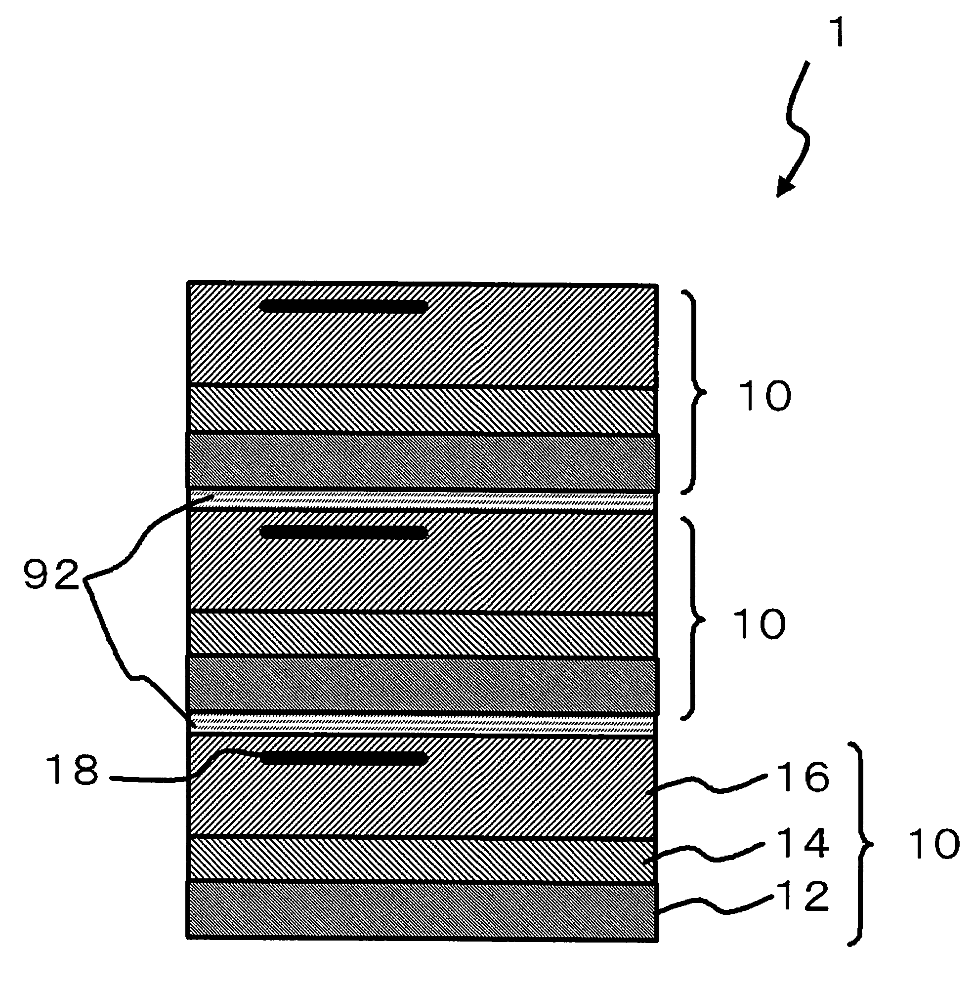
[0016]FIG. 1 is a cross-sectional view, showing first embodiment of a semiconductor device according to the present invention. A semiconductor device 1 includes a semiconductor chip 10. In the present embodiment, three semiconductor chips 10 are stacked. The semiconductor chips 10 are adhered with adhesive agents 92.

[0017]Each of the semiconductor chips 10 includes a semiconductor substrate 12, a semiconductor layer 14 and an interconnect layer 16. The semiconductor substrate 12 is, for example, a silicon substrate. The semiconductor substrate 12 has a specific resistance ρ1 (first specific resistance). A typical value of ρ1 is, for example, 1,000 Ωcm. Preferably, the specific resistance may be presented as: ρ1≧200 Ωcm, and more preferably, ρ1≧500 Ωcm.

[0018]A semiconductor layer 14 is provided on the semiconductor substrate 12. The semiconductor layer 14 is, for example, a silicon layer formed by an epitaxial growing process. Such semiconductor layer 14 exhibits a specific resistanc...

second embodiment

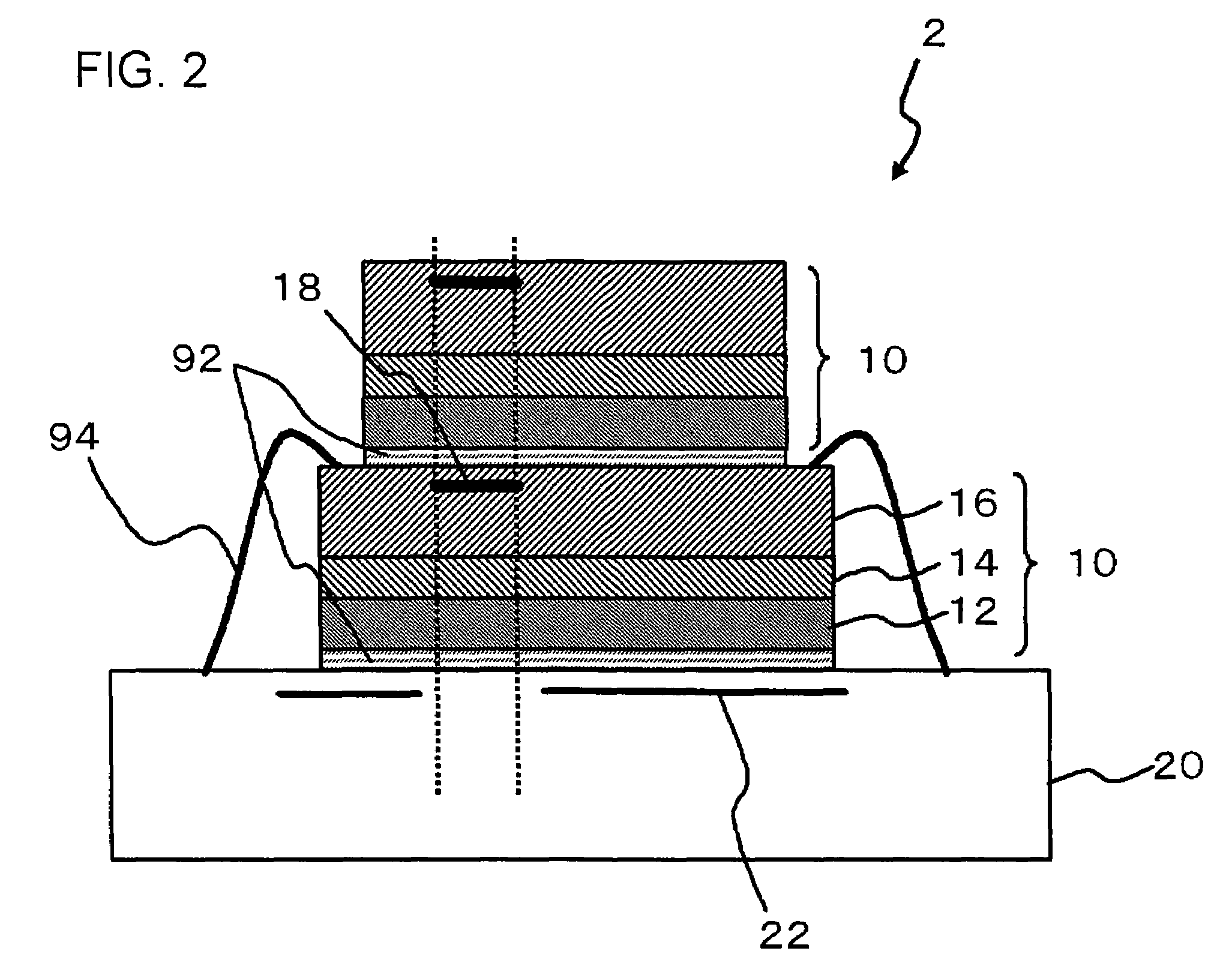
[0029]FIG. 2 is a cross-sectional view, showing second embodiment of a semiconductor device according to the present invention. A semiconductor device 2 comprises a semiconductor chip 10 and a printed circuit board 20. A configuration of the semiconductor chip 10 is equivalent to that described in reference to FIG. 1. In the present embodiment, two semiconductor chips 10 are stacked, and the semiconductor chip 10 in the bottom layer is attached to the printed circuit board 20 by a wire bonding. More specifically, the semiconductor chip 10 of the bottom layer is electrically coupled with the printed circuit board 20 by a wire 94. A coupling between the semiconductor chips 10 and a coupling of the semiconductor chip 10 with the printed circuit board 20 are achieved by the adhesive agent 92.

[0030]The interconnect 22 of the printed circuit board 20 is provided in a region that has no portion overlapping with the inductor 18 of the semiconductor chip 10 in plan view. More specifically, t...

third embodiment

[0032]FIG. 3 is a cross-sectional view, showing third embodiment of a semiconductor device according to the present invention. A semiconductor device 3 comprises a semiconductor chip 10 and a printed circuit board 20. A configuration of the semiconductor chip 10 is equivalent to that described in reference to FIG. 1. Further, a configuration of the printed circuit board 20 is equivalent to that described in reference to FIG. 2. In the present embodiment, two semiconductor chips 10 are stacked, and the semiconductor chip 10 in the bottom layer is attached to the printed circuit board 20 by a flip chip bonding. More specifically, the semiconductor chip 10 of the bottom layer is coupled to the printed circuit board 20 by a bump 30, in a situation that the interconnect layer 16 thereof is oriented toward the printed circuit board 20. Specifically, an electroconductive pad 42 (first pad) and an electroconductive pad 44 (second pad) are formed in each of the semiconductor chip 10 and the ...


PUM


Abstract

A semiconductor device 1 includes a semiconductor chip 10. Each of the semiconductor chips 10 includes a semiconductor substrate 12, a semiconductor layer 14 and an interconnect layer 16. The semiconductor substrate 12 has a specific resistance ρ1 (first specific resistance). A semiconductor layer 14 is provided on the semiconductor substrate 12. Such semiconductor layer 14 exhibits a specific resistance ρ2 (second specific resistance). The relationship of these specific resistances is: ρ2<ρ1. The interconnect layer 16 is provided on the semiconductor layer 14. An inductor 18 for transmitting and receiving signals with an external element outside the semiconductor chip 10 is provided in the interconnect layer 16.

Description

[0001]This application is based on Japanese patent application No. 2006-148,187, the content of which is incorporated hereinto by reference.BACKGROUND[0002]1. Technical Field[0003]The present invention relates to a semiconductor device.[0004]2. Related Art[0005]A plurality of semiconductor chip are deposited in a semiconductor device disclosed in Japanese Patent Laid-Open No. 2005-228,981. Each of the semiconductor chips is provided with an inductor for a communication. Each of the inductors are configured of an interconnect in an interconnect layer provided on the semiconductor substrate such as a silicon substrate and the like. The inductors are mutually inductively-coupled, which allows transmitting and receiving a signal between the chips.[0006]The present inventor has recognized as follows. In the above-described semiconductor device, an eddy current is generated in the semiconductor substrate by a magnetic field of the inductors. Then, according to Lenz's law, a new magnetic f...

Claims


Application Information

Patent Timeline
Patent Type & Authority Patents(United States)
IPC IPC(8): H01L27/02
CPCH01L23/48H01L25/0657H01L23/5227H01L24/48H01L2224/16225H01L2224/32145H01L2224/32225H01L2224/48091H01L2224/48227H01L2224/73204H01L2224/73265H01L2225/0651H01L2225/06517H01L2225/06527H01L2924/01079H01L2924/00014H01L2924/00H01L2924/00012H01L24/73H01L2224/05568H01L2224/05573H01L2924/14H01L2224/05599H01L2224/45099H01L2224/45015H01L2924/207
Inventor NAKASHIBA, YASUTAKA
Owner RENESAS ELECTRONICS CORP
Why Eureka
Try Eureka