photodiode

a photodiode and photodiode technology, applied in the field of photodiodes, can solve the problems of long travel distance of holes, difficult to satisfy the demands of difficulty in sufficiently alleviating the trade-off between increased sensitivity and speed, so as to achieve high-speed response, small width, and large specific resistance

Active Publication Date: 2009-06-11
FUJIFILM CORP +1
View PDF0 Cites 2 Cited by
  • Summary
  • Abstract
  • Description
  • Claims
  • Application Information

AI Technical Summary

Benefits of technology

[0022]Generally, a transparent electrode has a larger specific resistance in comparison with an opaque electrode, so that formation of a comb electrode only with transparent electrodes poses a problem that it becomes difficult to achieve a high-speed response. In contrast, in the photodiode of the present invention, an opaque electrode having a smaller specific resistance is formed on such a transparent electrode, so that the overall resistance of the comb electrode that includes these electrodes becomes small, and a high-speed response is realized. In addition, the opaque electrode has a smaller width than that of the transparent electrode, the area where light is blocked by the opaque electrode is very small, thereby high sensitivity is also ensured.

Problems solved by technology

Generally, in a photodiode having a transparent electrode, however, the sensitivity and high-speed response become a trade-off due to (1) a large time constant arising from a high resistance value, and (2) generation of low mobility holes even under the positive electrode if the active layer is an intrinsic or lightly doped N type layer, and the travel distance of the holes becomes long.
Further, in the structure described in U.S. Pat. No. 5,777,390, use of long transparent electrodes results in high resistance, so that it is difficult to sufficiently alleviate the trade-off between the increased sensitivity and speed.
That is, it is difficult to satisfy the demands of increased sensitivity and speed.
Still further, in the aforementioned structure, the transparency of the transparent electrode depends on the material, so that the transmittance is not freely (continuously) controlled.

Method used


Image

  • photodiode
  • photodiode
  • photodiode

Examples


Embodiment Construction

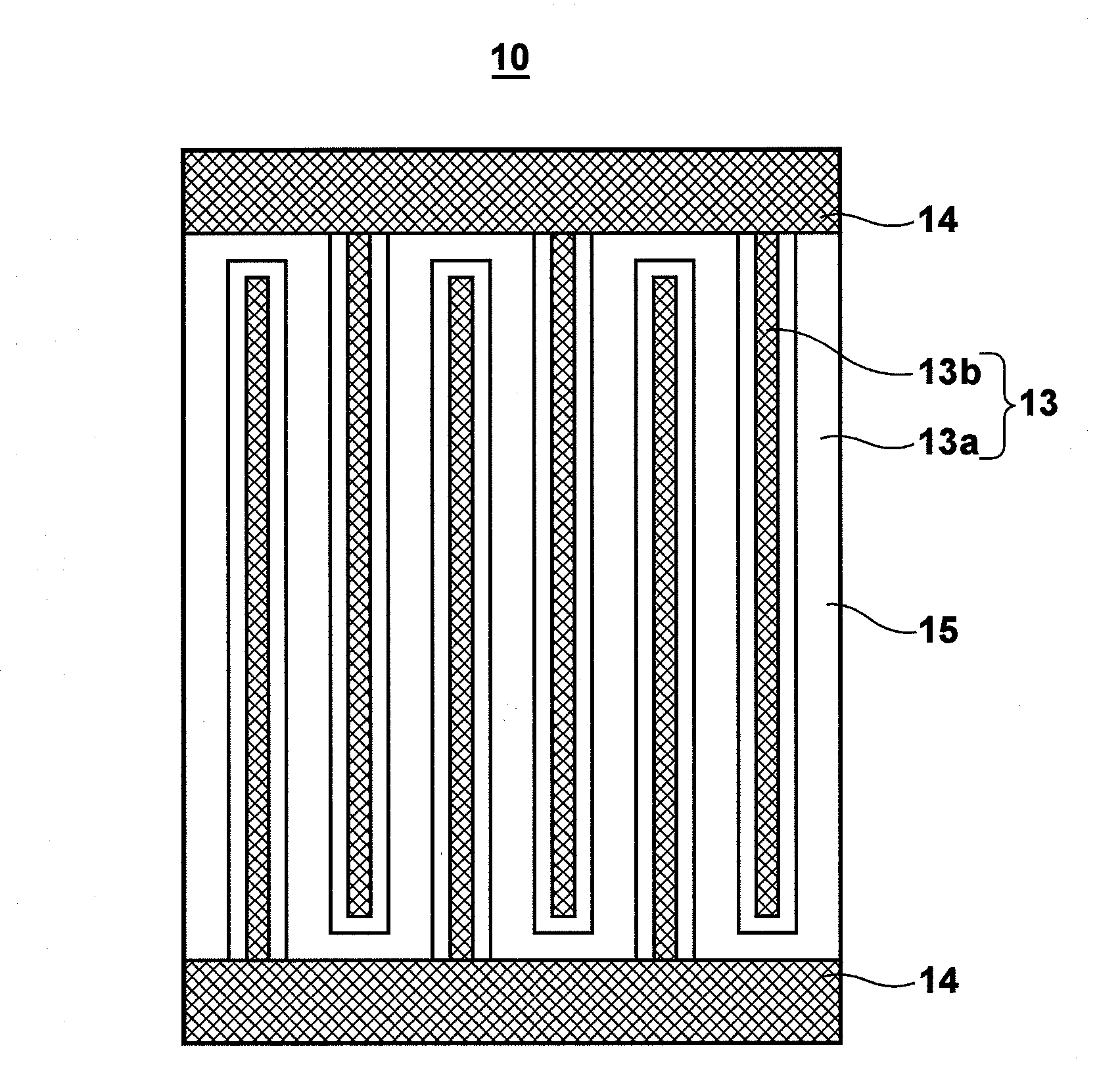
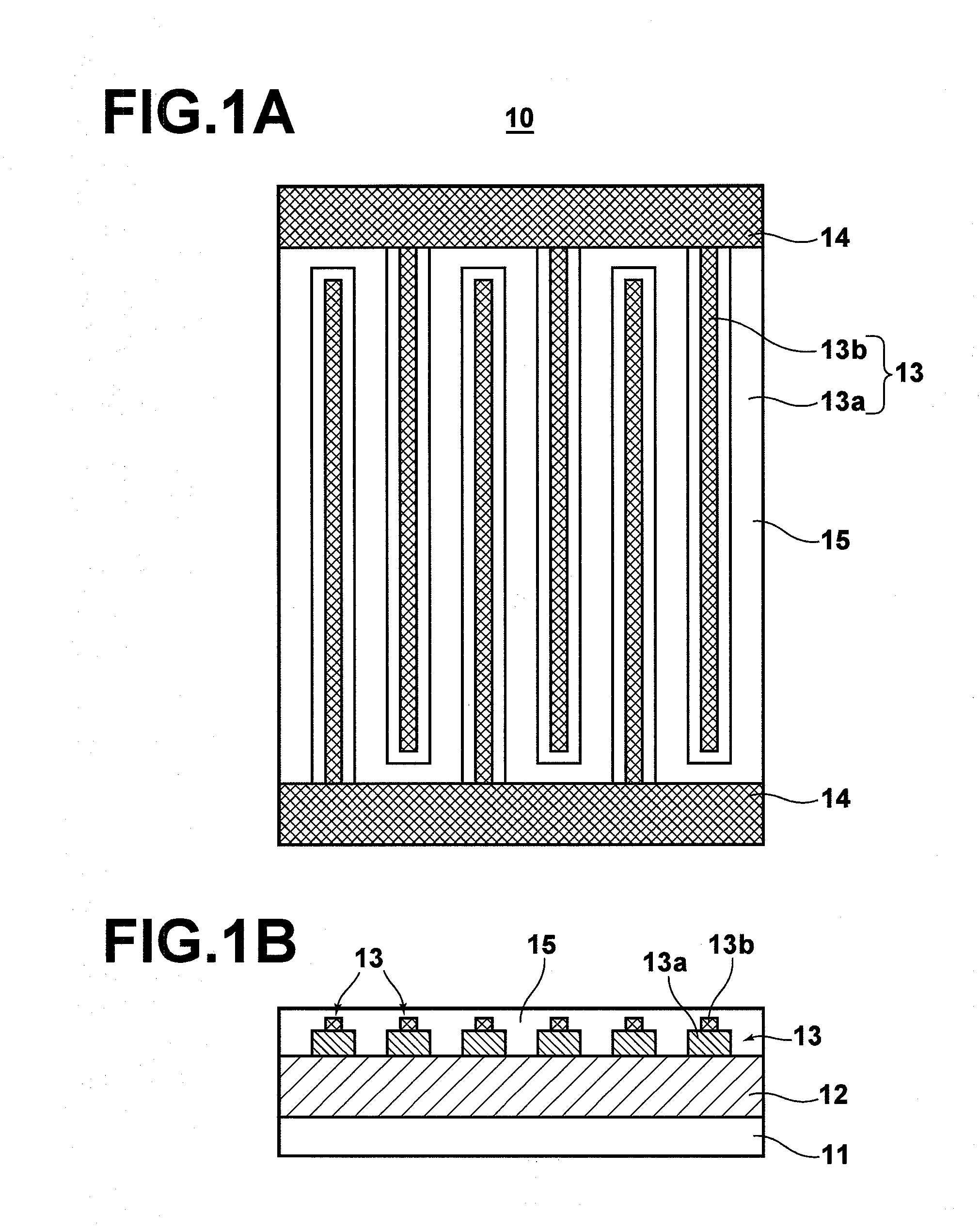
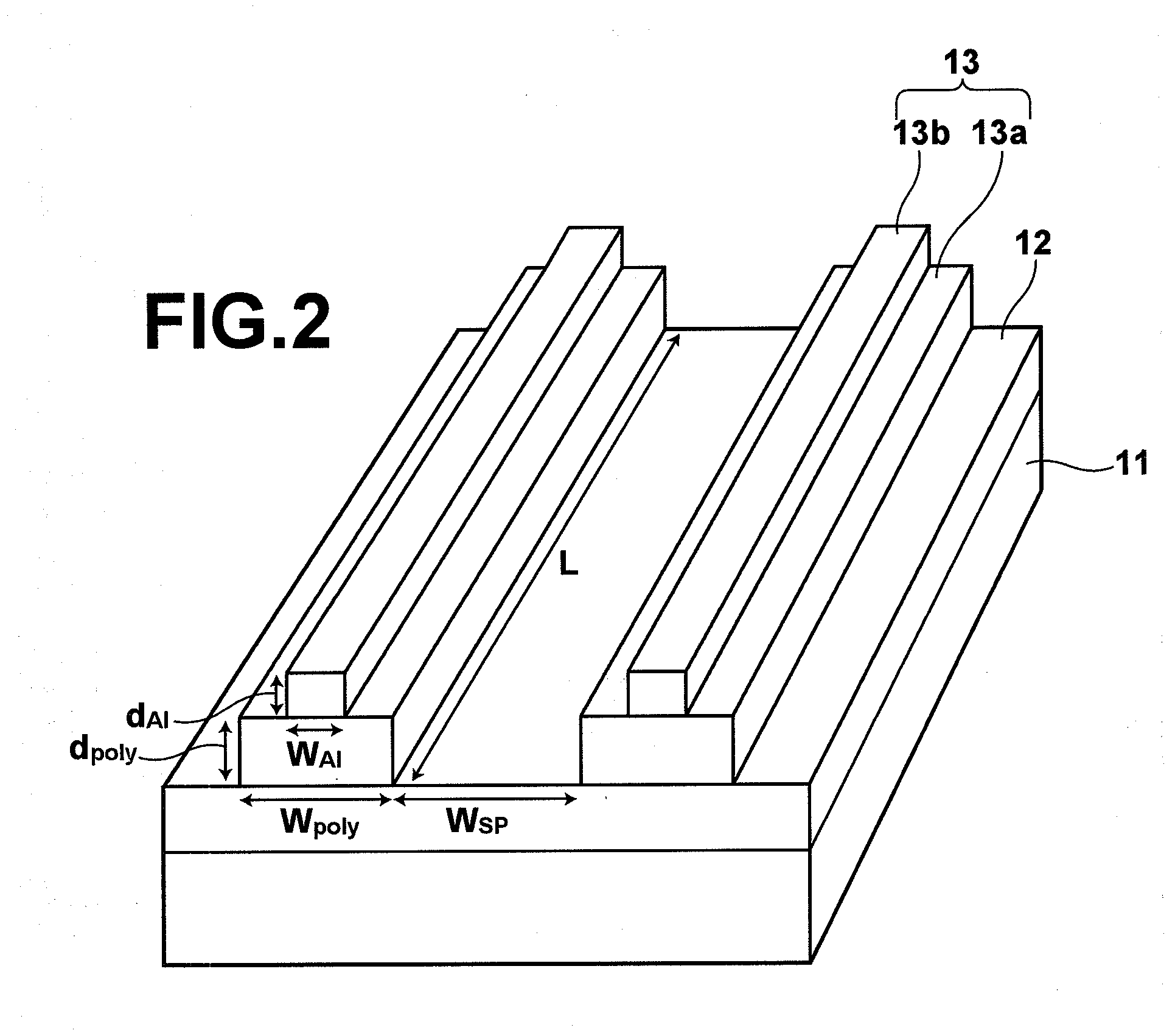
[0034]Hereinafter, an exemplary embodiment of the present invention will be described in detail with reference to the accompanying drawings. FIGS. 1A and 1B respectively illustrate a schematic planar shape and a schematic sectional elevational shape of the photodiode 10 according to an embodiment of the present invention. The photodiode of the present embodiment is, as an example, a MSM (metal-semiconductor-metal) lateral photodiode. As illustrated, the photodiode 10 includes: a semiconductor substrate 11; an active layer 12 formed on the substrate 11; a comb electrode including a plurality of comb electrode fingers 13 arranged side by side on the active layer 12 with appropriate spacing; electrodes 14 connected to the comb electrode fingers 13; and a passivation layer 15 formed on the comb electrode fingers 13.

[0035]In FIG. 1A, the upper electrode 14 is the positive electrode and connected to a signal line, and lower electrode 14 is the negative electrode and grounded. Thus, the co...


PUM


Abstract

A photodiode balanced in increased sensitivity and speed. The photodiode includes a semiconductor substrate, an active region formed on the semiconductor substrate, and a comb electrode connected to the active region. The comb electrode includes a plurality of electrode fingers, and each of the electrode fingers includes a transparent electrode contacting the active region, and an opaque electrode formed on the transparent electrode. Here, the width of the opaque electrode is set smaller than the width of the transparent electrode.

Description

BACKGROUND OF THE INVENTION[0001]1. Field of the Invention[0002]The present invention relates to a photodiode, and a method for manufacturing the same.[0003]2. Description of the Related Art[0004]Recently, in order to cope with a dramatic increase in the capacity of networks, epitomized by the widespread use of the Internet, development of high-speed optical transmission systems has been sought. Today, optical fibers having comparatively large apertures that facilitate alignment, such as plastic optical fibers, multimode glass optical fibers, and the like, are drawing increased attention as optical fibers for use not with trunk line systems but “last one mile” transmission systems, including subscriber line systems. As optical receivers suitable for high speed and large aperture optical fibers, MSM (metal-semiconductor-metal) photodiodes, lateral PIN photodiodes, and the like, in which electrodes are arranged laterally, i.e., in the direction parallel to the surface of the substrate...

Claims


Application Information

Patent Timeline
Patent Type & Authority Applications(United States)
IPC IPC(8): H01L23/482H01L21/00
CPCH01L31/022408H01L27/1446H01L31/085
Inventor MIYACHI, YUKIYAGIZIEWICZ, WOJCIECH P.MICHEL, JURGENKIMERLING, LIONEL C.
Owner FUJIFILM CORP
Why Eureka
Try Eureka