Pad and circuit board, electronic device using same

a technology of circuit boards and pads, applied in the field of surface mount technology, can solve the problems of limiting the application of bga, easy fracture of the soldering joint, and inability to ensure the quality of the soldering,

Active Publication Date: 2010-05-25
HON HAI PRECISION IND CO LTD
View PDF12 Cites 15 Cited by
  • Summary
  • Abstract
  • Description
  • Claims
  • Application Information

AI Technical Summary

Benefits of technology

[0008]In accordance with one embodiment, A pad for soldering a contact of a surface mounted component is provided herein. The pad includes a central portion and a plurality of separate extending portions extending from the central portion. All of the extending portions include a free end and a connected end connected to the central portion. A width of the free end is larger than a width of the connected end. A circuit board and an electronic device are also provided.

Problems solved by technology

However, one disadvantage of the BGA is that the solder balls of the BGA cannot flex in the way that longer leads can, and there is only one juncture between the solder balls and the pads, thus the solder joints fracture (solder-off) easily.
Another disadvantage is that once the BGA components are soldered, it is very difficult to detect soldering faults, thus, a quality of the soldering cannot be ensured.
These disadvantages which limits the application of BGA also occurs in other surface-mount packaging.
As a result, accurate positioning of the electronic elements cannot be assured, pseudo soldering, solder-off, and excess solder connections will also happen.

Method used


Image

  • Pad and circuit board, electronic device using same
  • Pad and circuit board, electronic device using same
  • Pad and circuit board, electronic device using same

Examples


Embodiment Construction

[0016]The embodiments will now be described in detail below with reference to the drawings.

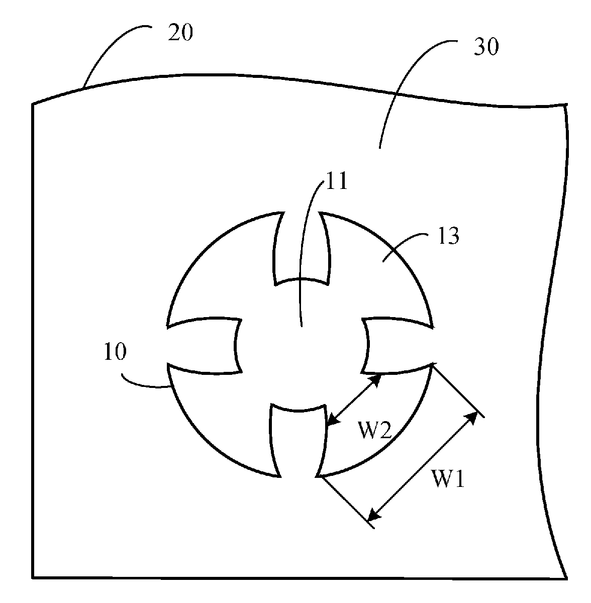
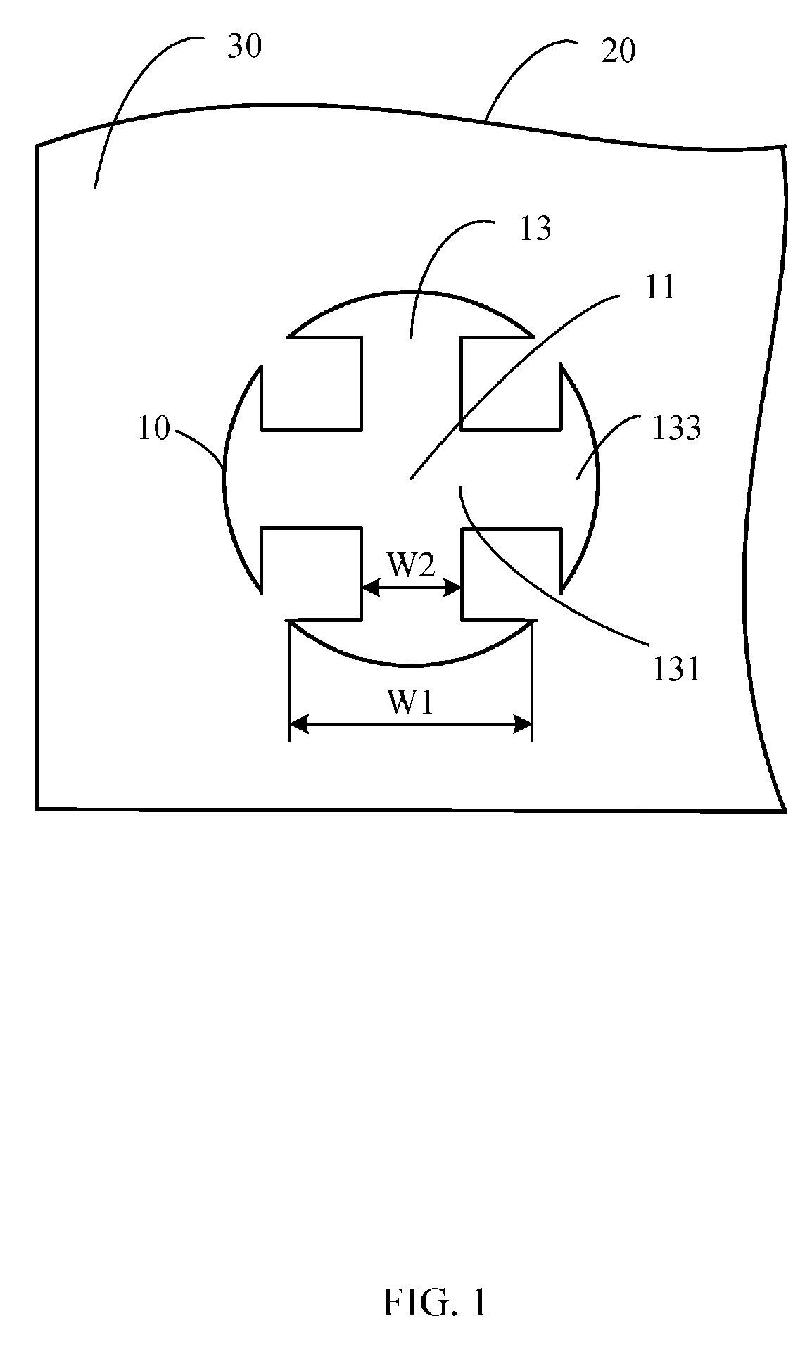
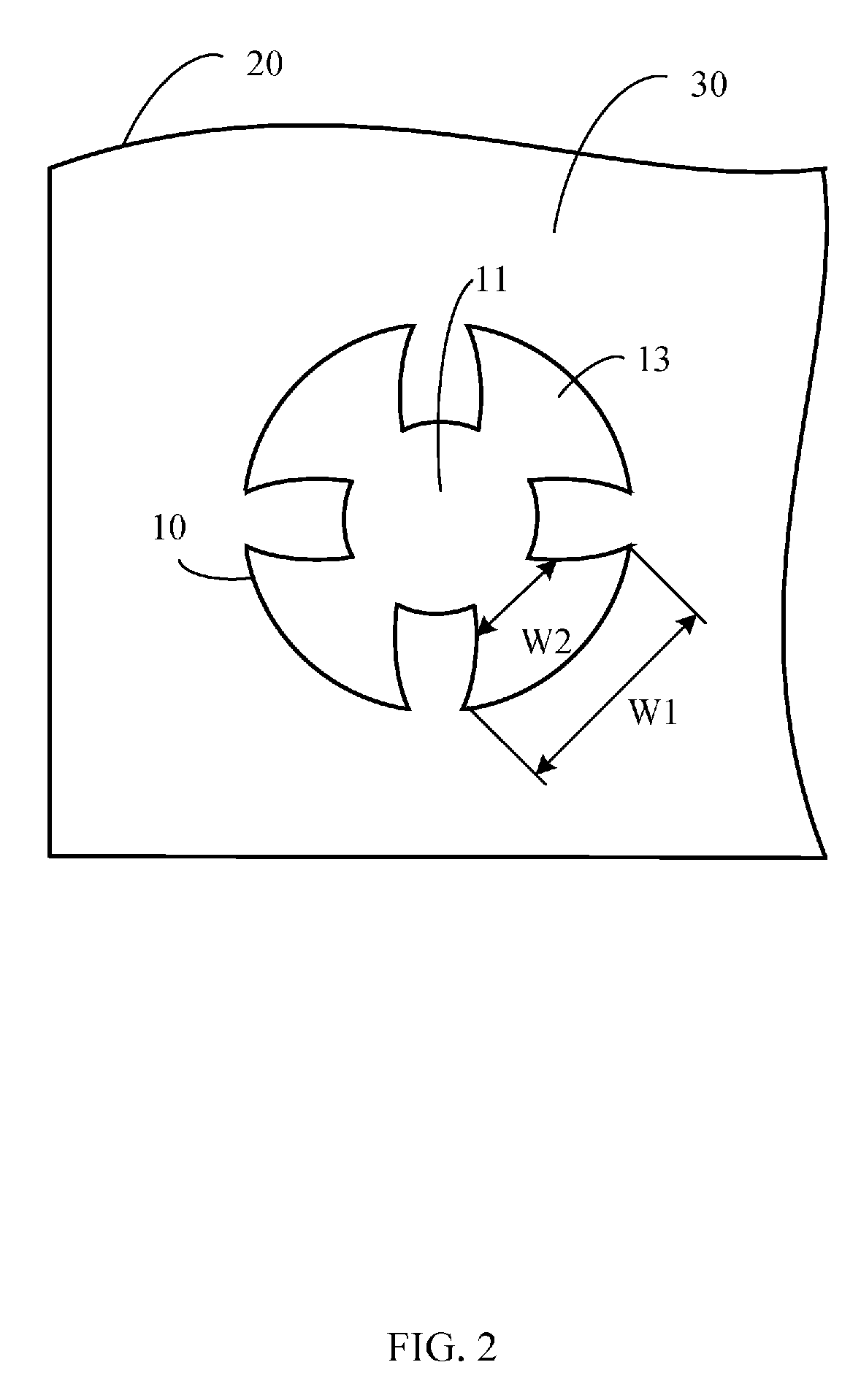
[0017]FIG. 1 is a partial top view of a circuit board 20 in accordance with a first exemplary embodiment. A pad 10 resides on a surface (not labeled) of the circuit board 20, and is surrounded by a solder resist 30 that also resides on the surface of the circuit board 20. The solder resist 30 extends to a periphery of the pad 10. The pads 10 can be formed on the circuit board 20 by chemical etching etc, and a solder paste may be printed onto the pad 10.

[0018]The circuit board 20 may be a printed circuit board laminate composed of multiple layers of non-conductive material and conductive traces sandwiched together to form a rigid planar structure. The pad 10 is electrically connected to the conductive traces of the circuit board 20 and is configured for mounting a contact of a surface mounted component (SMC, a resistor, a capacitor, an integrated circuit, an image sensor or the like, for exampl...


PUM


Abstract

A pad for soldering a contact of a surface mounted component is provided herein. The pad includes a central portion and a plurality of separate extending portions extending from the central portion. All of the plurality of separate extending portions includes a free end and a connected end connected to the central portion. A width of the free end is larger than a width of the connected end. A circuit board and an electronic device are also provided.

Description

BACKGROUND[0001]1. Technical Field[0002]The present invention relates to surface mount technology (SMT), and more particularly, to an improved pad used for mounting a surface mounted component (SMC) on a circuit board.[0003]2. Description of Related Art[0004]In recent years, surface mount technology (SMT) is being widely used in electronic device manufacturing. SMT is a method for assembling surface mounted components (SMC) onto the surface of printed circuit boards (PCBs). A pin or solder ball of a SMC is usually smaller than its leaded counterpart because it has either smaller leads or no leads at all. It may have short pins or leads of various styles, flat contacts, a matrix of balls (ball grid arrays, BGAs, for example), or terminations on the body of the component.[0005]Ball grid arrays (BGA) accommodates the demands of SMT, and resolves the applications with high density, lower thermal resistance, low inductance leads, improved high speed performances, multiple functions, and ...

Claims


Application Information

Patent Timeline
Patent Type & Authority Patents(United States)
IPC IPC(8): H01L23/48
CPCH05K1/111H01L2224/16225H05K3/3436H05K2201/09381Y02P70/611H05K2201/10734Y10T428/24942Y10T428/12222H05K2201/094Y02P70/50
Inventor TSAI, SHU-JENCHEN, LONG-FONGTSENG, WEN-HAWWONG, SHIH-FANG
Owner HON HAI PRECISION IND CO LTD
Why Eureka
Try Eureka