Level shift circuit and method for the same

a level shift circuit and level shift technology, applied in logic circuits, logic circuit coupling/interface arrangements, pulse techniques, etc., can solve the problem of slow output level switching speed, achieve speed up level switching, and speed up output level switching

Inactive Publication Date: 2010-06-01
RICHTEK TECH
View PDF3 Cites 8 Cited by
  • Summary
  • Abstract
  • Description
  • Claims
  • Application Information

AI Technical Summary

Benefits of technology

[0011]A first objective of the present invention is to provide a level shift circuit with faster output level switching, in which a pulse generator generates a pulse according to the level switching at a node, and the pulse drives a latch circuit to generate the desired output.
[0012]A second objective of the present invention is to provide a level shift circuit which speeds up the output level switching by speeding up the level switching at a node.
[0013]A third objective of the present invention is to provide a method to achieve faster output level switching in a level shift circuit.

Problems solved by technology

All the above-mentioned prior art circuits have a common drawback: their output level switching speed is slow.

Method used


Image

  • Level shift circuit and method for the same
  • Level shift circuit and method for the same
  • Level shift circuit and method for the same

Examples


first embodiment

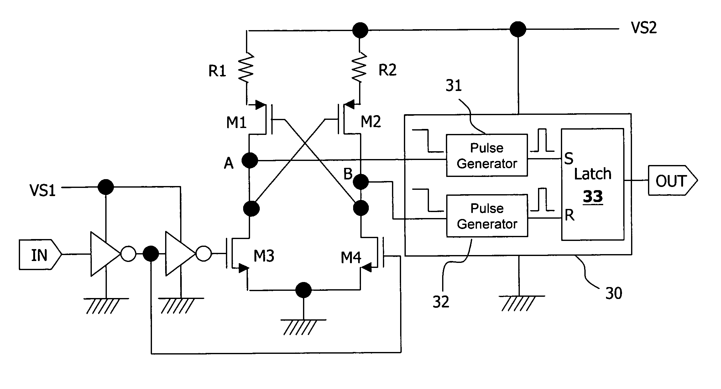
[0029]FIG. 6 schematically shows a first embodiment according to the present invention. As shown in the figure, a level shift circuit comprises a pair of PMOS transistors M1 and M2, and a pair of NMOS transistors M3 and M4 (the PMOS and NMOS pairs constituting a basic level shift circuit 10). In addition to the above, the level shift circuit according to this embodiment further comprises an output circuit 30. The output circuit 30 includes pulse generators 31 and 32, and a latch circuit 33. The pulse generator 31 generates a pulse according to the falling edge of the signal at the node A. The pulse is received by the set input S of the latch circuit 33 so that the latch circuit 33 outputs a signal of high level. Likely, the pulse generator 32 generates a pulse according to the falling edge of the signal at the node B; the pulse is received by the reset input R of the latch circuit 33 so that the latch circuit 33 outputs a signal of low level. The output circuit 30 operates between a...

second embodiment

[0031]FIG. 7 shows the present invention. As shown in the figure, besides the basic level shift circuit 20, the level shift circuit further includes an output circuit 40. The output circuit 40 includes pulse generators 41 and 42, and a latch circuit 43. The pulse generator 41 generates a pulse according to the rising edge of the signal at the node A; the pulse is received by the set input S of the latch circuit 43 so that the latch circuit 43 outputs a signal of high level. Likely, the pulse generator 42 generates a pulse according to the rising edge of the signal at the node B; the pulse is received by the reset input R of the latch circuit 43 so that the latch circuit 43 outputs a signal of low level. The output circuit 40 operates between a high level which is the first high operational voltage VS1 and a low level which is VG2, so its output signal has a high level of VS1 and a low level of VG2, which are exactly the desired signal levels to be shifted to by the level shift circu...

third embodiment

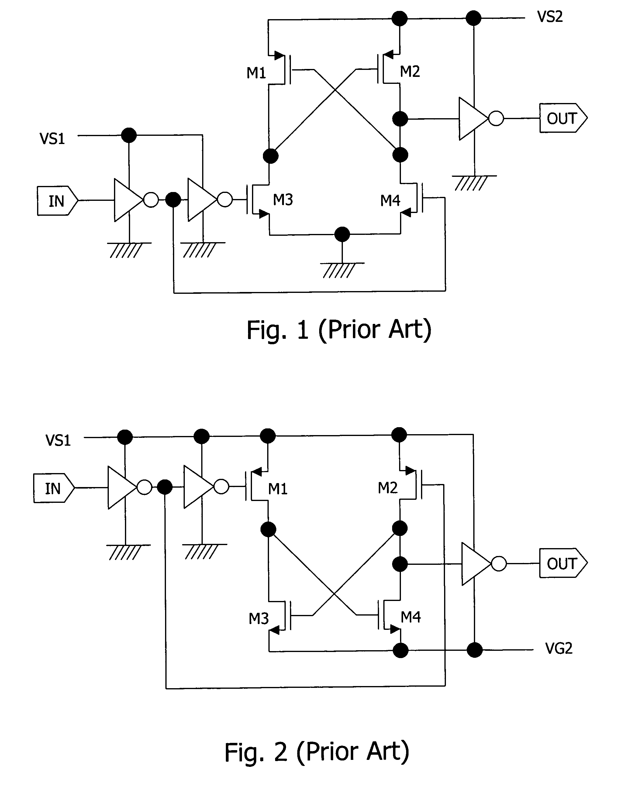
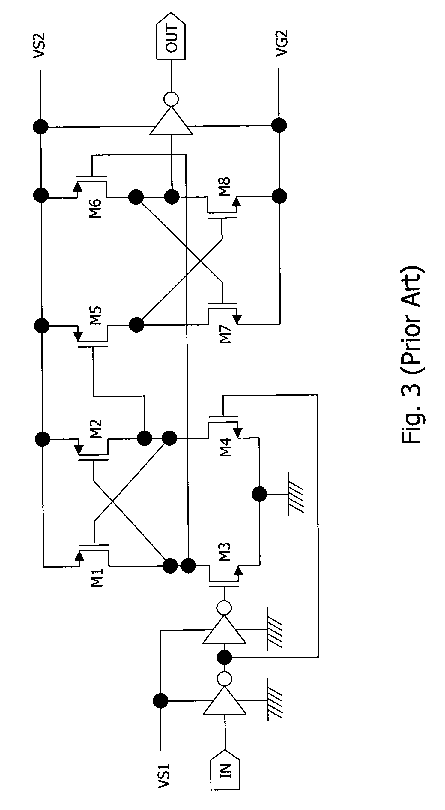
[0033]FIG. 8 shows the present invention. The purpose of this circuit is to shift the signal levels from VS1 / 0V to VS2 / VG2. Note that in this embodiment, it does not require two basic level shift circuits (eight transistors) as that shown in FIG. 3, but only requires one basic level shift circuit with four transistors (either one of the basic level shift circuits 10 and 20, shown to be the basic level shift circuit 10 in the figure). The output circuit 50 operates between a high level which is VS2 and a low level which is VG2, so that its output signal has a high level of VS2 and a low level of VG2, which are exactly the desired signal levels to be shifted to by the level shift circuit.

[0034]The embodiments of FIGS. 6-8 explain the first concept of the present invention, i.e., by the level switching of the voltage signal at a critical node, which is much faster, a pulse is generated to drive a latch circuit, so that an output signal is capable of switching its levels in a much short...


PUM


Abstract

The present invention discloses a level shift circuit which comprises: a basic level shift circuit for receiving inputs of first high and low operational voltage levels and generating outputs of second low and high operational voltage levels at a first node; and an output circuit for outputting a signal of one of the second operational voltage levels according to a voltage level switching at the first node.

Description

BACKGROUND OF THE INVENTION[0001]1. Field of the Invention[0002]The present invention relates to a level shift circuit, and in particular to a level shift circuit with faster output level switching, and a method for the same.[0003]2. Description of the Related Art[0004]A power control circuit chip often requires a level shift circuit to convert one DC voltage level to another. The conversion may increase the voltage difference between the high and low levels, decrease the voltage difference between the high and low levels, or shift the high and low levels to different voltages without changing the voltage difference between them. FIGS. 1-3 respectively show three examples:[0005]The circuit of FIG. 1 converts VS1 / 0V (high / low level of an input signal) to VS2 / 0V (high / low level of an output signal), and usually VS2>VS1. VS1 and VS2 for example may be 1.5V and 3.3V, respectively. Sometimes the circuit is also used in the case where VS2<VS1. The low level of the input signal and t...

Claims


Application Information

Patent Timeline
Patent Type & Authority Patents(United States)
IPC IPC(8): H03K19/094H03K5/00
CPCH03K3/35613H03K3/012
Inventor CHIANG, YUN-CHI
Owner RICHTEK TECH
Why Eureka
Try Eureka