Simultaneous grain modulation for BEOL applications

a technology of simultaneous grain modulation and beol, which is applied in the direction of semiconductor devices, semiconductor/solid-state device details, electrical apparatus, etc., can solve the problems of double manufacturing cost and difficult limitation of single cu grain size for interconnects embedded within the same insulating layer, so as to reduce semiconductor manufacturing costs and eliminate unnecessary processing steps. , the effect of reducing the manufacturing processing steps

Inactive Publication Date: 2010-06-08
GLOBALFOUNDRIES INC
View PDF13 Cites 28 Cited by
  • Summary
  • Abstract
  • Description
  • Claims
  • Application Information

AI Technical Summary

Benefits of technology

[0011]A first embodiment is directed to a semiconductor structure comprising a first and second opening, a barrier material, a copper grain promotion material, a copper seed, and electroplated copper. The first and second opening are within the same insulating layer. A barrier material is deposited on the insulating layer in the first and second opening. A copper grain promotion material is deposited on the barrier material of the first opening. A copper seed is deposited on the copper grain promotion material of the first opening and on the barrier material of the second opening. Copper is electroplated on the copper seed within the first and second openings. The copper grain promotion material increases grain size of the electroplated copper in the first opening, such that an average grain size of the electroplated copper grown in the first opening is larger than an average grain size of the electroplated copper in the second opening. The first and second opening are within the same insulating level layer.
[0013]The invention solves the aforementioned problems associated with Cu interconnects embedded within the same insulating layer level. More specifically, the invention enables the creation of Cu interconnects embedded within the same insulating layer level with divergent Cu grain sizes. In so doing, the present invention enables the creation of Cu interconnects embedded within the same insulating layer level that perform most efficiently for the intended application of the Cu interconnect. In addition, semiconductor manufacturing processing steps are reduced in half because multiple insulating layer levels are not required to create Cu interconnects with different Cu grain sizes. Finally, the elimination of unnecessary processing steps reduces semiconductor manufacturing costs by at least fifty percent.

Problems solved by technology

One problem encountered in semiconductor manufacturing is the manufacture of copper (Cu) interconnects within the same insulating level layer with different Cu grain sizes.
The limitation of a single Cu grain size for interconnects embedded within the same insulating layer is problematic because, for certain applications Cu interconnects perform more advantageously with a smaller Cu grain size, while for other applications Cu interconnects perform more advantageously with a larger Cu grain size.
In addition, creation of a new layer of Cu interconnects with a different Cu grain size, doubles manufacturing costs.

Method used


Image

  • Simultaneous grain modulation for BEOL applications
  • Simultaneous grain modulation for BEOL applications
  • Simultaneous grain modulation for BEOL applications

Examples


Embodiment Construction

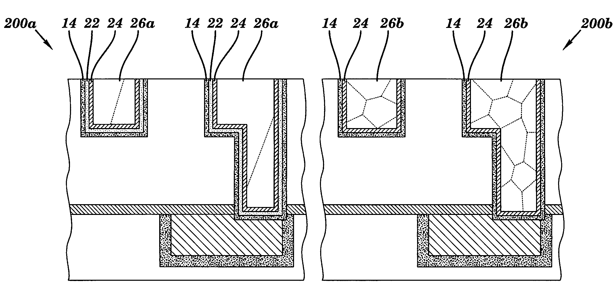
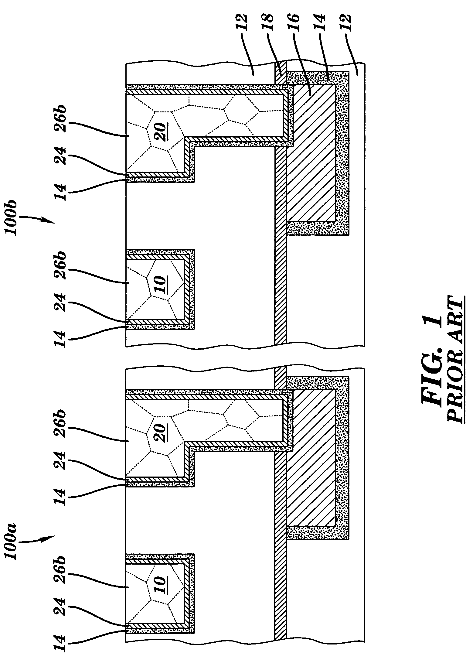
[0018]The invention will now be described with reference to the accompanying figures. In the figures, various aspects of the structures have been depicted and schematically represented in a simplified manner to more clearly describe and illustrate the invention.

[0019]By way of overview and introduction, the embodiments of the invention are directed to a Cu interconnect and a method for creating the same. The invention enables a Cu interconnect embedded within the same insulating layer level to have a different Cu grain size than another Cu interconnect embedded within the same insulating layer level.

[0020]The invention will be described with reference to the FIGS. 2-6, which depict the formation of an improved semiconductor structure.

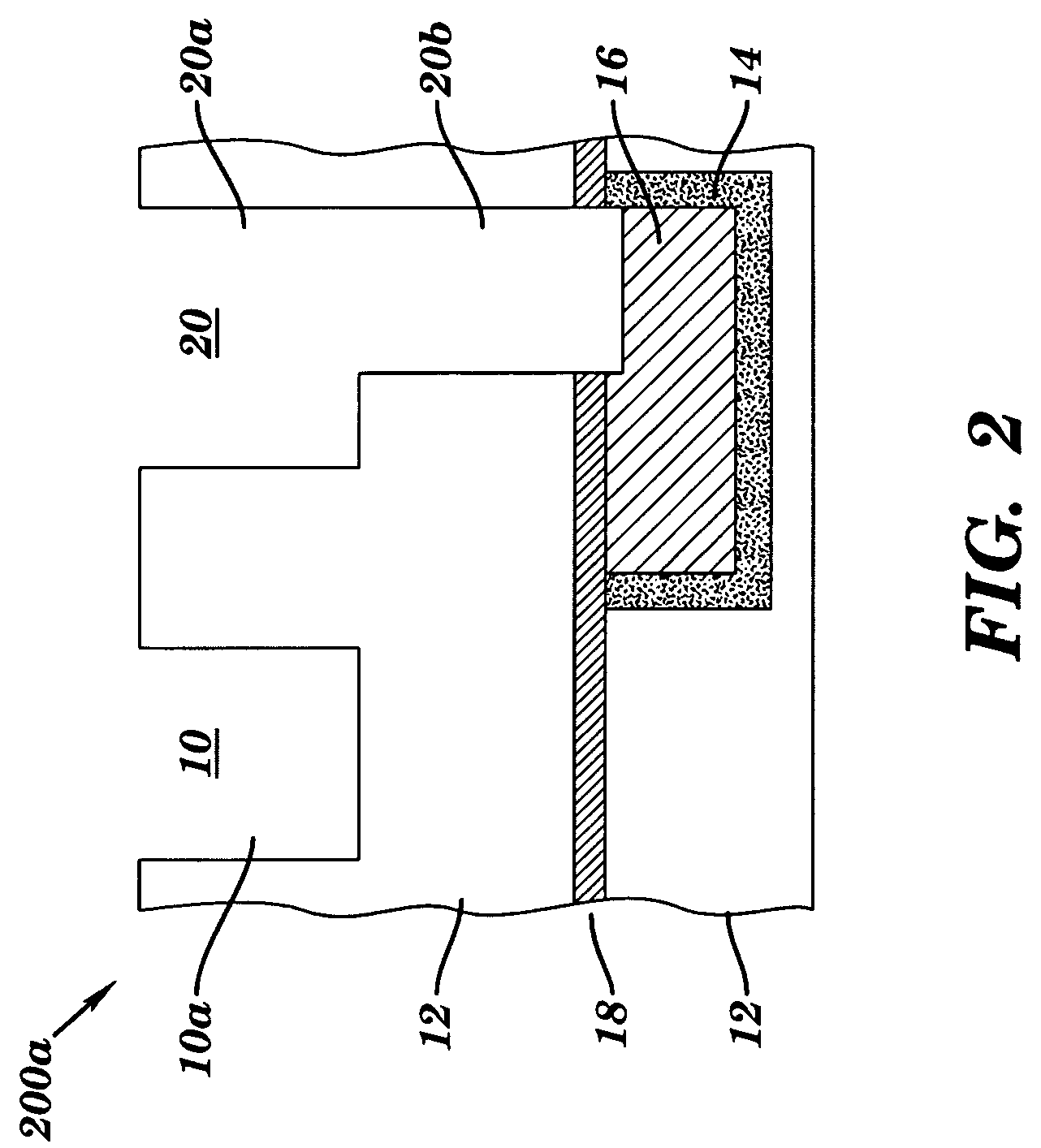
[0021]FIG. 2 depicts the first step of the method of the present invention. More specifically, FIG. 2 demonstrates the formation of a first opening 200a and second opening 200b (not shown until FIG. 4) in an insulating layer 12. Note that the openings 2...


PUM

PropertyMeasurementUnit
grain sizeaaaaaaaaaa
semiconductor structureaaaaaaaaaa
semiconductoraaaaaaaaaa

Abstract

The invention is directed to an improved semiconductor structure, such that within the same insulating layer, Cu interconnects embedded within the same insulating level layer have a different Cu grain size than other Cu interconnects embedded within the same insulating level layer.

Description

BACKGROUND OF THE INVENTION[0001]1. Field of the Invention[0002]The invention relates generally to a semiconductor structure, and more particularly to copper (Cu) interconnects embedded in the same insulating level layer with different copper grain sizes.[0003]2. Description of the Related Art[0004]One problem encountered in semiconductor manufacturing is the manufacture of copper (Cu) interconnects within the same insulating level layer with different Cu grain sizes. Currently, Cu interconnects formed within the same insulating level layer comprise the same Cu grain size. The limitation of a single Cu grain size for interconnects embedded within the same insulating layer is problematic because, for certain applications Cu interconnects perform more advantageously with a smaller Cu grain size, while for other applications Cu interconnects perform more advantageously with a larger Cu grain size. For example, a large Cu grain size results in lower electrical resistivity and longer ele...

Claims


Application Information

Patent Timeline
Patent Type & Authority Patents(United States)
IPC IPC(8): H01L29/40
CPCH01L23/5226H01L23/53238H01L23/53233H01L2924/0002H01L2924/00
Inventor YANG, CHIH-CHAOHSU, LOUIS C.JOSHI, RAJIV V.
Owner GLOBALFOUNDRIES INC
Why Eureka
Try Eureka