Transmitting apparatus

a technology of transmitting apparatus and transmission device, which is applied in the direction of logic circuit coupling/interface arrangement, pulse technique, baseband system details, etc., can solve the problems of increasing the bit error rate obtained at the time of reception, easy and easy reception error on the receiving apparatus side. , to achieve the effect of preventing the fluctuation of common mode potential and reducing the common mode potential

Active Publication Date: 2010-06-08
THINE ELECTRONICS
View PDF7 Cites 11 Cited by
  • Summary
  • Abstract
  • Description
  • Claims
  • Application Information

AI Technical Summary

Benefits of technology

[0012]It is preferred that the pre-emphasis buffer circuit further have a voltage-holding circuit that keeps a potential of a connection point (referred to as “first connection point” hereinafter) between the first current source and the switch circuit constant, and keeps a potential of a connection point (referred to as “second connection point”) between the second current source and the switch circuit constant, during the third time interval. In this case, during the third time interval in which the outputs of the pre-emphasis buffer circuit are in the high-impedance state, the voltage-holding circuit keeps the potential of the connection point between the first current source and the switch circuit (first connection point) constant, and keeps the potential of the connection point between the second current source and the switch circuit (second connection point) constant, thus stabilization of the common mode potential can be achieved.
[0014]It is preferred that resistance values of the first resistor and second resistor provided in the voltage-holding circuit be twice a value of terminating resistance of the differential transmission lines. Also, preferably, a resistance value that is obtained when each of the fifth through eighth switches is in an on-state is twice a resistance value obtained when each of the first through fourth switches is in the on-state. In this case, when the outputs of the pre-emphasis buffer circuit are in any state, the potentials of the first connection point and the second connection point become substantially constant, thus even when an output state fluctuates, the fluctuation of the common mode potential can be diminished.
[0015]According to the present invention, fluctuation of the common mode potential can be prevented and high-speed, long-distance signal transmission can be performed.

Problems solved by technology

Incidentally, when performing high-speed, long-distance signal transmission, a problem arises in which the bit error rate obtained at the time of reception is increased due to attenuation of the AC component of a signal in the differential transmission lines.
Specifically, when the level of a digital signal to be transmitted is inverted and thereby the directions of the current signals that are output from the first output terminal and second output terminal of the transmitting apparatus are inverted, it requires time for the magnitude of the current signals to reach a predetermined value after the inversion, and, as a result, a reception error easily occurs on the receiving apparatus side.
Since the transmitting apparatus performs both current control and voltage control, a problem arises in which the common mode potential fluctuates easily and EMI (electromagnetic interference) noise increases due to a phenomenon in which the current signal loops back via the differential transmission lines and terminating resistors.

Method used


Image

  • Transmitting apparatus
  • Transmitting apparatus
  • Transmitting apparatus

Examples


Embodiment Construction

[0047]Hereinafter, the best mode for carrying out the present invention is described in detail with reference to the attached drawings. It should be noted that the same reference numerals are assigned to the same elements in the explanations of the drawings, and redundant explanations are omitted.

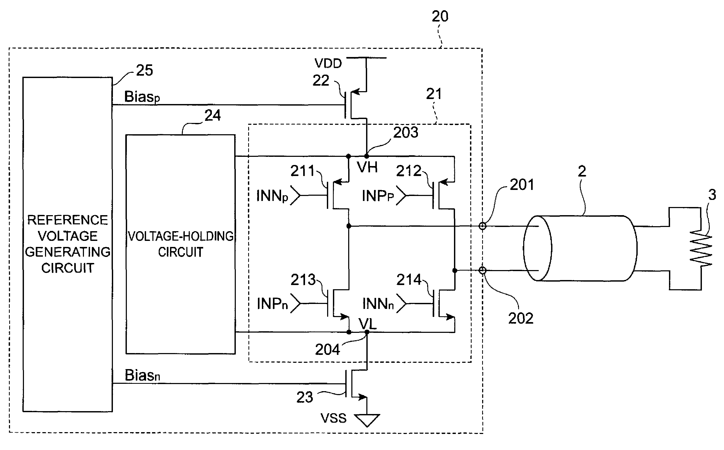
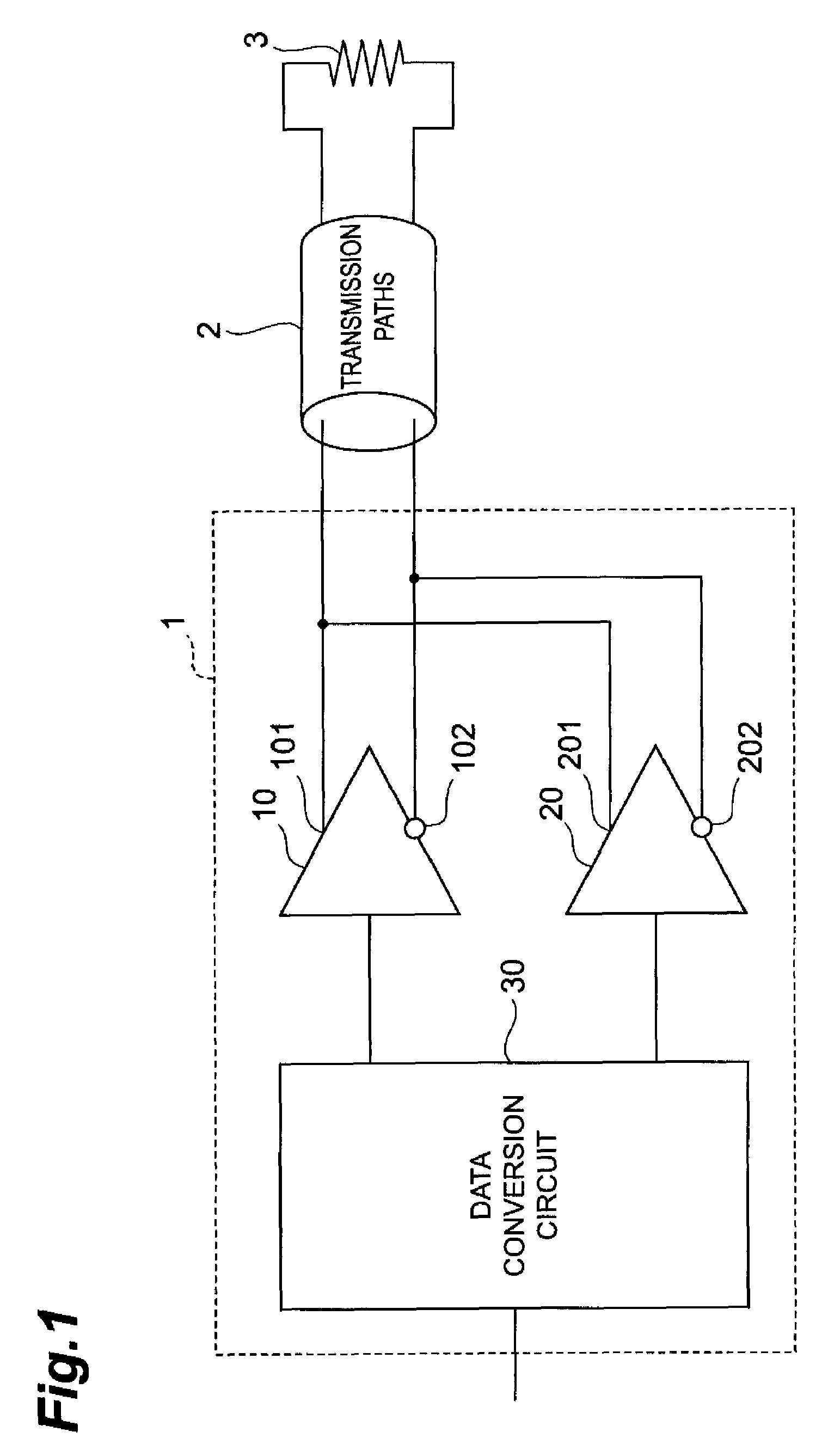
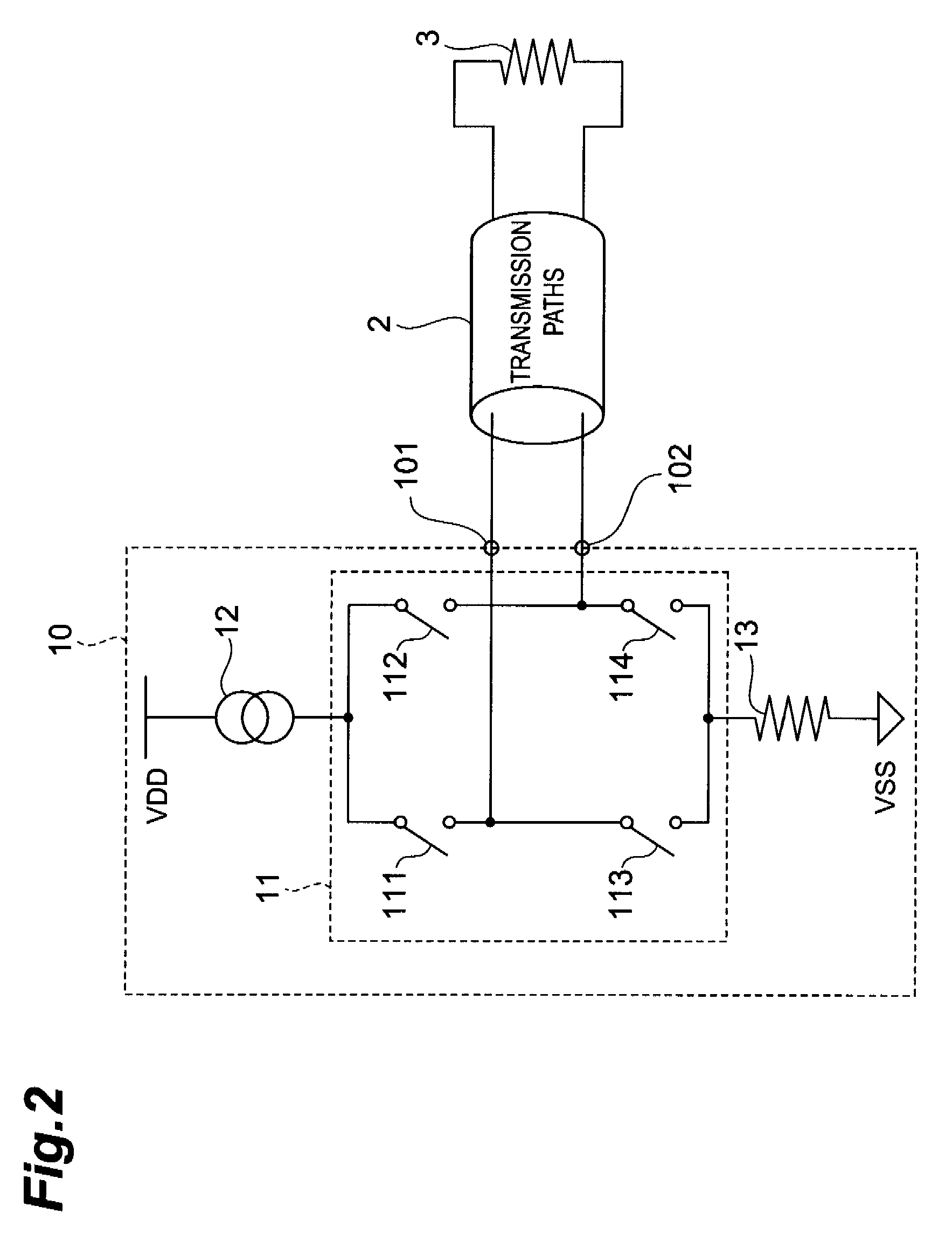
[0048]First of all, a schematic configuration of the transmitting apparatus 1 according to the present embodiment is described using FIG. 1 through FIG. 3. FIG. 1 is a schematic configuration diagram of the transmitting apparatus 1 according to the present embodiment. FIG. 2 is a schematic diagram of the main buffer circuit 10 provided in the transmitting apparatus 1 according to the present embodiment. FIG. 3 is a schematic diagram of the pre-emphasis buffer circuit 20 provided in the transmitting apparatus 1 according to the present embodiment. It should be noted that these drawings show a pair of differential transmission lines 2 to which the transmitting apparatus 1 outputs current sign...


PUM


Abstract

To provide a transmitting apparatus capable of suppressing the fluctuation of a common mode potential and performing high-speed, long-distance signal transmission. The transmitting apparatus has a main buffer circuit and a pre-emphasis buffer circuit 20. The pre-emphasis buffer circuit 20, which has a switch circuit 21, a first current source 22, and a second current source 23, uses the switch circuit 21 to output a current signal having the same direction as an output current of the main buffer circuit 10 during a certain time interval starting from a time point when the level of data to be transmitted changes, and brings the output terminals 201, 202 to a High-Z state during a time interval when the level is constant after a lapse of the abovementioned certain time interval. The output of the pre-emphasis buffer circuit 20 has no influence on the common mode potential of the output of the main buffer circuit but has influence only the amplitude of the current signal output to a differential transmission line. In this manner, the transmitting apparatus can suppress the fluctuation of the common mode potential and can perform high-speed, long-distance signal transmission.

Description

TECHNICAL FIELD[0001]The present invention relates to a transmitting apparatus that can be used suitably in a low-voltage differential signaling (LVDS) system for transmitting and receiving a digital signal by changing the directions of a current flowing in a pair of resistor-terminated differential transmission lines.BACKGROUND ART[0002]LVDS, which is standardized as IEEEP1596, 3, is used for transmitting a digital signal by changing the directions of a current flowing in a pair of resistor-terminated differential transmission lines, and is generally capable of transmitting the digital signals at high speed and with low power consumption and less noise.[0003]A transmitting apparatus that is used in LVDS has a first output terminal and a second output terminal that are connected to a pair of differential transmission lines, wherein when a digital signal to be transmitted is at an H level, a current signal flowing from the first output terminal to the second output terminal via the p...

Claims


Application Information

Patent Timeline
Patent Type & Authority Patents(United States)
IPC IPC(8): H03K19/094H03K19/0175
CPCH04L25/0282H03K17/6872H04L25/0272H03K19/0175H04L25/03H04L25/02
Inventor MIURA, SATOSHI
Owner THINE ELECTRONICS
Why Eureka
Try Eureka