Dual-phosphor flat panel radiation detector

a radiation detector and flat panel technology, applied in the field of radiation detectors, can solve the problems of degrading the sharpness of the obtained radiation image, deteriorating the visible light detection efficiency of the photodetector, and reducing the sharpness of the image, so as to reduce the thickness of the substrate, and reduce the distance between the surfaces

Active Publication Date: 2010-06-29
FUJIFILM CORP
View PDF16 Cites 168 Cited by
  • Summary
  • Abstract
  • Description
  • Claims
  • Application Information

AI Technical Summary

Benefits of technology

[0021]The radiation detector of the present invention includes: two scintillator layers that convert irradiated radiation to light; and a solid state photodetector that detects the light converted by the two scintillator layers and converts the detected light to electrical signals, the solid state detector being disposed between the two scintillators. Here, the scattering length of each of the scintillators is not greater than 100 μm for the light propagating in the direction parallel to the surface of the scintillator. Thus, the average rectilinear propagation distance of light scattered in the direction parallel to the surface of the scintillator is small in each scintillator, so that the dispersion of the light in the direction parallel to the surface of the scintillator may be prevented, thereby the sharpness of the obtained radiation image may be improved.
[0023]If the solid state photodetector is a photodetector constituted by a thin film transistor and a photoconductive layer layered on top of another, or arranged in a planar fashion, the structure described above may be realized, and the light from the two scintillators may be used effectively.
[0024]Here, if the thin film transistors are thin film transistors formed on a substrate and peel transferred from the substrate, the thickness of the solid state photodetector disposed between the two scintillator layers may be reduced by removing the substrate. This may reduce the distance between the surfaces of the two scintillator layers facing each other.
[0025]Further, if the thin film transistors are thin film transistors with the substrate, on which the thin film transistor is formed, being thinned or removed by a chemical dissolution method or a polishing method, the thickness of the solid state photodetector disposed between the two scintillator layers may be reduced by reducing the thickness of the substrate. This may reduce the distance between the surfaces of the two scintillator layers facing each other.
[0026]Still further, if the thin film transistors are thin film transistors formed on a substrate peelably disposed on a support and peeled off the support together with the substrate, the thickness of the solid state photodetector disposed between the two scintillator layers may be reduced by reducing the thickness of the substrate peelably disposed on the support. This may reduce the distance between the surfaces of the two scintillator layers facing each other.
[0027]In particular, if the thin film transistors are transparent, the light irradiated thereon from the two scintillators may also be used effectively, so that the image quality may be further improved.

Problems solved by technology

Consequently, the visible light detection efficiency of the photodetector is deteriorated, and the sharpness of the obtained radiation image is degraded.
Further, the rear light receiving surface of the solid state photodetector viewed from the direction from which the radiation is irradiated is arranged such that it invariably receives fluorescence transmitted through the substrate, so that the fluorescence is dispersed while transmitting through the substrate, causing a problem of degraded image sharpness.
Thus, the visible light converted by the fluorescent glass substrate is spread within the substrate, causing a problem of degraded sharpness of obtained radiation images.

Method used


Image

  • Dual-phosphor flat panel radiation detector
  • Dual-phosphor flat panel radiation detector
  • Dual-phosphor flat panel radiation detector

Examples


Embodiment Construction

[0031]Hereinafter, an exemplary embodiment of the present invention will be described with reference to accompanying drawings.

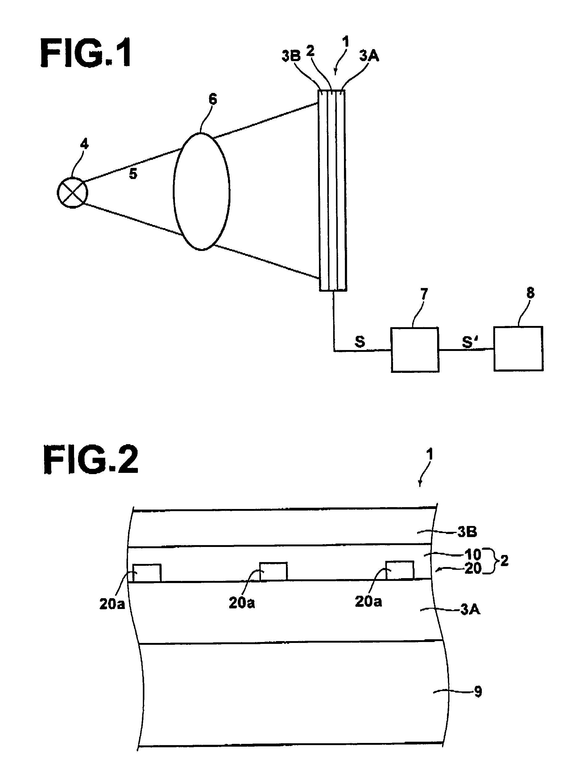
[0032]FIG. 1 is a drawing illustrating an embodiment of the radiation detector of the present invention. As shown in FIG. 1, a radiation detector 1 of the present embodiment includes the following layers layered in the order listed below: a first scintillator 3A, a solid state photodetector 2, and a second scintillator 3B. Thus, the solid state photodetector 2 is disposed between the two scintillator layers 3A, 3B in sandwiched manner.

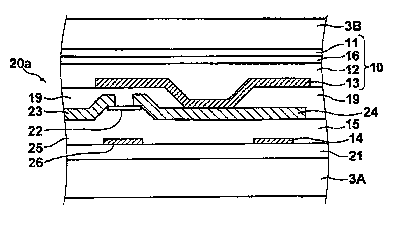
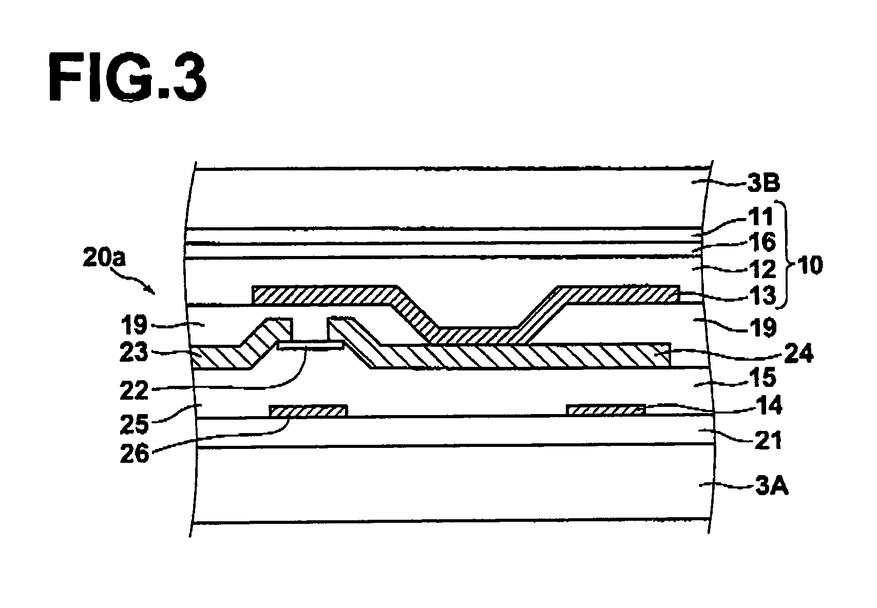
[0033]As shown in FIG. 2, the radiation detector 1 includes a base 9 on which the first scintillator 3A, solid state photodetector 2, and second scintillator 33 are layered. The solid state photodetector 2 includes: a photoconductive section 10 formed of a photoconductive layer 12 and a thin film transistor layer 20 layered on top of another. The thin film transistor layer 20 is a layer in which multitudes of thin film transisto...


PUM


Abstract

A solid state radiation detector capable of improving the sharpness of obtained radiation images. The solid state radiation detector includes: two scintillator layers that convert irradiated radiation to light; and a solid state photodetector, disposed between the two scintillators, that detects the light converted by the two scintillator layers and converts the detected light to electrical signals. Here, the scattering length of each of the scintillators is not greater than 100 μm for the light propagating in the direction parallel to the surface of the scintillator.

Description

BACKGROUND OF THE INVENTION[0001]1. Field of the Invention[0002]The present invention relates to a radiation detector, more specifically, to a radiation detector that employs a combination of scintillator and solid state photodetector.[0003]2. Description of the Related Art[0004]Radiation detectors formed of a solid state photodetector and a scintillator, which converts radiation to visible light, layered on top of another are proposed as described, for example, in Japanese Unexamined Patent Publication Nos. 59(1984)-211263 and 2(1990)-164067, U.S. Pat. No. 5,187,396, and “Signal, noise, and readout considerations in the development of amorphous silicon photodiode arrays for radiotherapy and diagnostic x-ray imaging”, L. E. Antonuk et al., SPIE, Vol. 1443, pp. 108-119, 1991. The solid state photodetector includes, for example, a substrate made of silica glass with a thickness of 3 mm on which a transparent conductive layer and a conductive layer are formed with an amorphous semicond...

Claims


Application Information

Patent Timeline
Patent Type & Authority Patents(United States)
IPC IPC(8): G01T1/20
CPCH01L27/14676H01L27/14663
Inventor TAKAHASHI, KENJI
Owner FUJIFILM CORP
Why Eureka
Try Eureka