Electroformed stencils for solar cell front side metallization

a solar cell and front side metallization technology, applied in the direction of photomechanical equipment, originals for photomechanical treatment, instruments, etc., can solve the problems of loss of line definition, ragged edges, and obstructed metallization ink flow

Active Publication Date: 2010-07-06
FRY S METALS INC
View PDF12 Cites 46 Cited by
  • Summary
  • Abstract
  • Description
  • Claims
  • Application Information

AI Technical Summary

Benefits of technology

[0017]One or more methods according to the present disclosure may further comprise removing the stencil, while leaving the conductive ink substantially adhered to the semiconductor substrate. The conductive ink may adhere to the semiconductor substrate without significant bleedout, such that at least one line of conductive ink deposited on the semiconductor substrate has substantially straight edges.
[0026]Further disclosed herein is a method of forming a stencil for semiconductor metallization comprising providing a photosensitive plate including a base plate and a layer of photoresist, the layer of photoresist being between approximately 50 micrometers and 150 micrometers thick, applying an optical separator above the photosensitive plate, the optical separator being transparent to ultraviolet light and having a thickness of between ten micrometers and one millimeter, applying a photolithography mask above the optical separator, passing ultraviolet light through the photolithography mask and optical separator and onto the photosensitive plate, whereby an image characterized by a taper is formed in the layer of photoresist by cross-linking of the photoresist exposed to the ultraviolet light through the photolithography mask and optical separator, removing non-exposed photoresist from the photosensitive plate, forming a stencil on the base plate by electroforming, and removing the stencil from the base plate. The stencil formed exhibits exceptionally flat bottom surfaces and exceptionally sharp edges at a corner of a bottom of a wall of an aperture formed in the stencil such that a stencil is capable of printing conductive ink onto a semiconductor substrate without significant bleedout.

Problems solved by technology

There are several well-known difficulties associated with printing conductive metallization ink with a screen printer onto an electronic substrate or solar cell.
For example, the metallization ink flow may be obstructed by the carrier mesh.
Another difficulty may be the loss of line definition and resultant ragged edges caused by the mesh, which deteriorates over time because of the wear of the emulsion screen.
Yet another difficulty is the screen printer's inability to print small line widths due to bleeding of the metallization ink at the contact interface between the screen and the substrate.
A further difficulty is the screen printer's inability to print high aspect ratio features because of bleeding of the metallization ink at the contact interface between the screen and the substrate or because of slumping of the ink, leading to widened and topped-off lines.
However, changing the rheology of the metallization ink to a more viscous type does not adequately solve these problems as the screen may clog very easily when a more viscous ink is used.
However, most stencils, such as those used in the electronics assembly industry, typically exhibit significant bleeding and subsequent line broadening and irregularity when used to deposit metallization ink, or other less viscous materials, on semiconductor substrates, making them generally unsuitable for such an application.
When imaging thick photoresist layers, e.g., 100 micrometers, through a mask by a collimated light source, such as a Tamarack 161 collimated exposure system, the resist structure typically shows a tapered form with an angle of about 6 degrees, with the top of the image being smaller than the bottom, thereby limiting the resolution of narrow lines.

Method used


Image

  • Electroformed stencils for solar cell front side metallization
  • Electroformed stencils for solar cell front side metallization
  • Electroformed stencils for solar cell front side metallization

Examples


examples

Baseline Tests

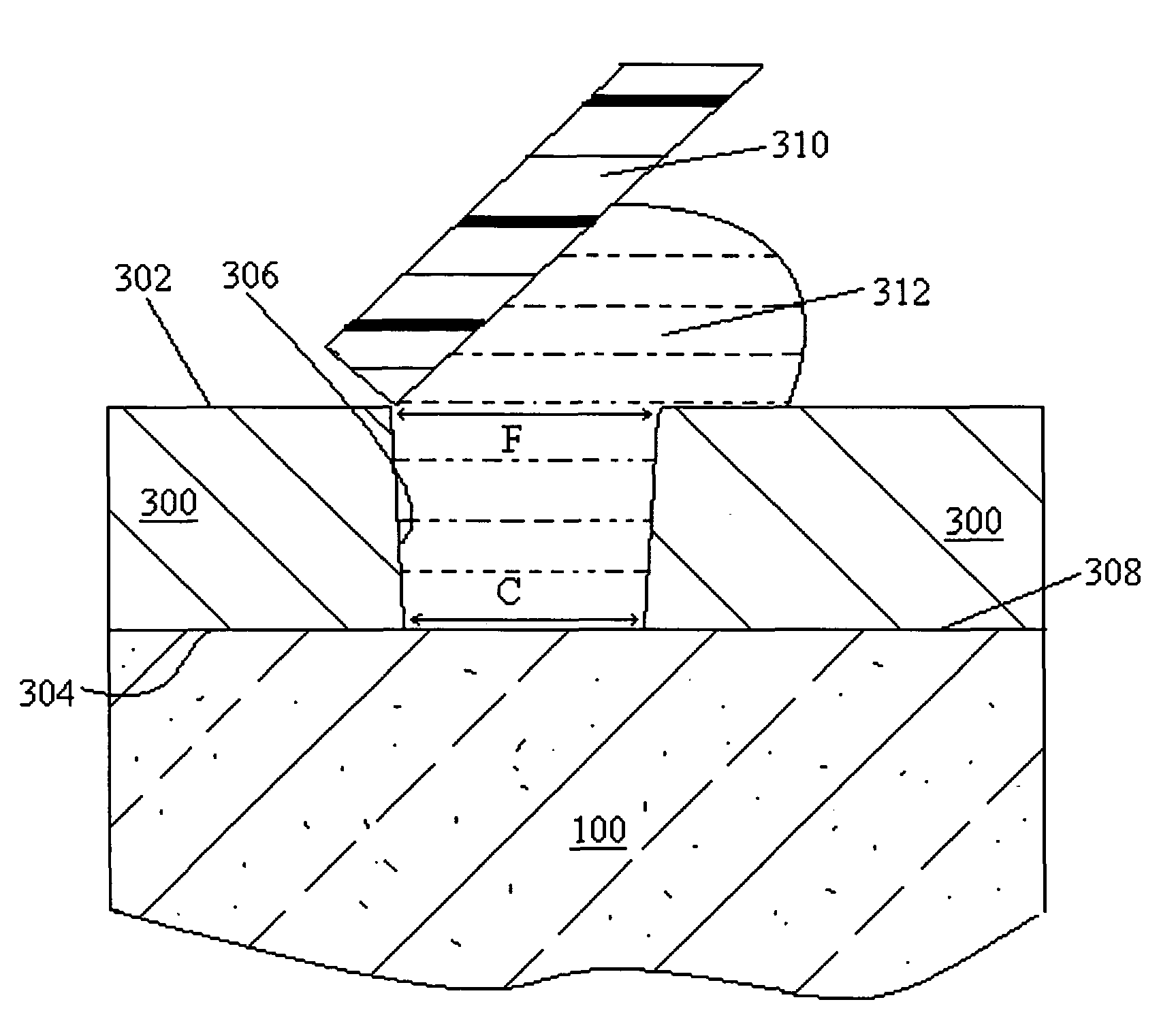
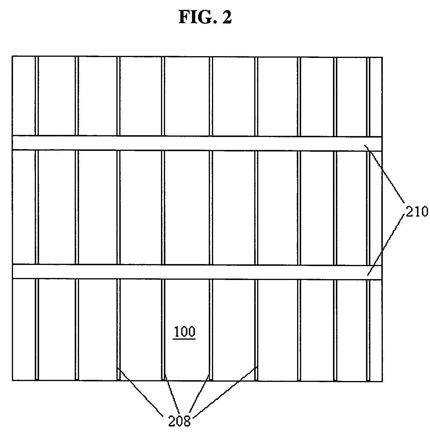
[0069]Tests were performed on laser cut stainless steel stencils with various dimensions, including 70 and 90 micrometer wide openings in 70 micrometer thick sheets. Two layouts were tested, one with and one without a busbar included. The busbar was in the form of a two mm wide opening connecting all of the fingers. Both layouts had, in total, 52 parallel lines.

[0070]The laser cut of the apertures varied in width, with wider and narrower areas. Some openings were sometimes as narrow as 35 micrometers, in which printing was feasible. The laser cut was relatively rough, most likely causing observed darker spots in the print due to difficulties with paste release. The design incorporating the busbar was impossible to print due to paste drop-out. The lines at the cell extremities were much wider than those near the center. Line thickness was acceptable; about 60 micrometers high when dried.

[0071]Testing was also performed on electroformed nickel stencils. Larger screens (1...


PUM


Abstract

A method for providing metallization upon a semiconductor substrate utilizing a stencil having at least one aperture extending from the contact side to the fill side, the contact side of the stencil being substantially flat and forming a sharp edge with a wall of the at least one aperture, the at least one aperture being tapered such that an area of a cross-section of the at least one aperture at the fill side is larger than an area of the cross-section of the at least one aperture at the contact side. A method of forming a stencil for depositing metallization lines on a semiconductor substrate is also disclosed.

Description

RELATED APPLICATION[0001]This application claims priority under 35 U.S.C. §119(e) to U.S. Provisional Application Ser. No. 60 / 973,957, entitled “ELECTROFORMED STENCILS FOR SOLAR CELL FRONT SIDE METALLIZATION,” filed on Sep. 20, 2007, which is herein incorporated by reference in its entirety for all purposes.BACKGROUND OF INVENTION[0002]1. Field of Invention[0003]The current disclosure is directed to apparatus and methods of printing features on substrates, such as conductive features on semiconductor substrates, and more specifically, to the printing of metallization contact lines on the surfaces of photovoltaic devices, as well as to methods for forming stencils for performing semiconductor metallization processes.[0004]2. Discussion of Related Art[0005]In solar cells, front side metallization allows charge built up on a front surface of a solar cell during use to be transported away from the cell and used to provide electrical power. This front side metallization is deposited on t...

Claims


Application Information

Patent Timeline
Patent Type & Authority Patents(United States)
IPC IPC(8): H01L21/02
CPCB41M3/006G03F7/0015G03F7/12G03F7/2014H01L31/022425H05K3/1225Y02E10/50
Inventor MEEUS, THOMASKORSSE, HANSBHATKAL, RAVINDRA M.
Owner FRY S METALS INC
Why Eureka
Try Eureka