
Epitaxial substrate for field effect transistor

a field effect transistor and epitaxial substrate technology, which is applied in the direction of semiconductor devices, semiconductor device details, electrical apparatuses, etc., can solve the problems of gate leakage current increase and pinch-off characteristic degradation

Active Publication Date: 2010-07-06
SUMITOMO CHEM CO LTD +1
View PDF4 Cites 15 Cited by
  • Summary
  • Abstract
  • Description
  • Claims
  • Application Information

AI Technical Summary

Benefits of technology

[0024]The present invention allows micropipes existing in the SiC single crystal base substrate to be closed, and provides a nitride-based epitaxial growth semiconductor crystal for a field effect transistor having good characteristics, and therefore, has an extreme significance in the industrial use.

Problems solved by technology

Thus, there has existed a problem that the GaN-FET formed by using such a crystal has significantly impaired element characteristics such as lead to a short-circuit, an increase in gate leak current and degradation in pinch-off characteristic.

Method used


Image

  • Epitaxial substrate for field effect transistor
  • Epitaxial substrate for field effect transistor
  • Epitaxial substrate for field effect transistor

Examples


example 1

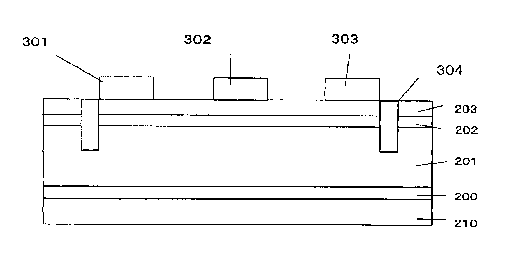
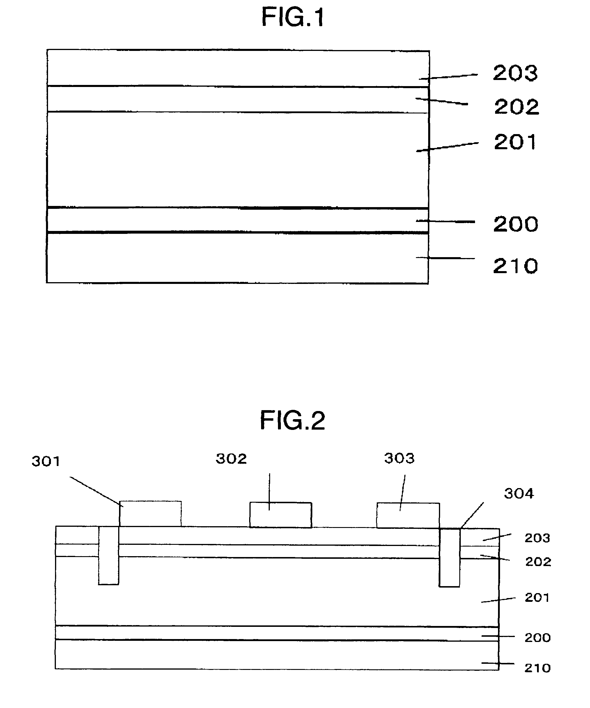
[0055]Using an MOCVD apparatus, a SiC substrate having a density of about 30 micropipes / cm2 was heated to 600° C. for growing an AlN buffer layer to a thickness of 2000 Å.

[0056]Then the temperature of the substrate was changed to (1) 950° C., (2) 1050° C. and (3) 1150° C. for stacking an GaN micropipe closing layer to a thickness of 2 μm.

[0057]Then, after the substrate temperature was allowed to fall to about a room temperature, the substrate was removed from the reactor. The substrates which had been subjected to (1), (2) and (3) were observed by using a cross-Nicol image generated by transmitted light from an optical microscope in order to identify a position of a micropipe within the substrates, and subsequently, the light was changed to epi-illumination in order to determine whether the above described micropipes were spread to the surface of the micropipe closing layer or was closed in the micropipe closing layer.

[0058]The closing rate was determined by the following equation:

(...

example 2

[0060]Using an MOCVD apparatus, a SiC substrate having a density of about 30 micropipes / cm2 was heated to 600° C. for growing an AlN buffer layer to a thickness of 2000 Å.

[0061]Then a temperature of the substrate was changed to 1150° C. for stacking a GaN micropipe closing layer to at thickness of 2 μm. And then the temperature of the substrate was changed to 1050° C. for growing an undoped-GaN channel layer to a thickness of 5000 Å.

[0062]Subsequently, undoped-AlGaN whose Al composition ratio was 0.25 was grown to a thickness of 250 Å. Then, after the substrate temperature was allowed to fall to about room temperature, the substrate was removed from the reactor.

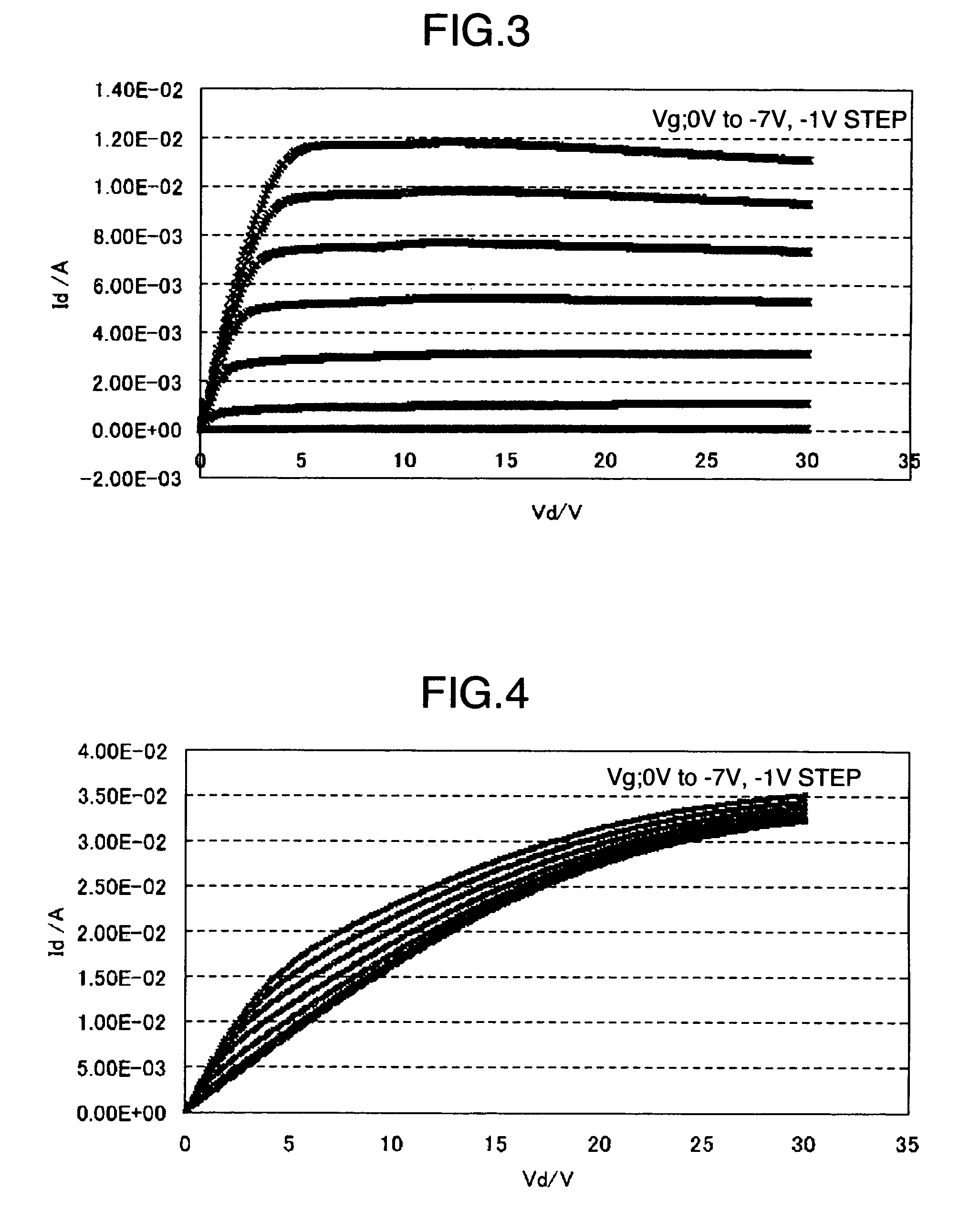
[0063]After confirming that the micropipe within the substrate was closed with respect to the obtained sample, a resist pattern was formed so as to be in alignment such that a gate was located immediately on the closed micropipe by the use of photolithography. Subsequently, N+ ion implantation was performed to provide a devic...


PUM


Abstract

An epitaxial crystal for a field effect transistor which has a nitride-based III-V group semiconductor epitaxial crystal grown on a SiC single crystal base substrate having micropipes by use of an epitaxial growth method, wherein at least a part of the micropipes spreading from the SiC single crystal base substrate into the epitaxial crystal terminate between an active layer of the transistor and the SiC single crystal base substrate.

Description

BACKGROUND OF THE INVENTION[0001](1) Field of the Invention[0002]The present invention relates to a nitride-based III-V group semiconductor epitaxial crystal for a field effect transistor.[0003](2) Description of the Related Art[0004]A field effect transistor using a nitride-based III-V group semiconductor epitaxial substrate (hereinafter referred to as a GaN-FET) is a field effect transistor driven by using a GaN layer as a channel layer, and is a device which has been rapidly attracting attention in recent years for its use in high-frequency and power device applications, because this transistor has a high breakdown voltage and a higher heat-resisting property, and also each component of this transistor has a lower impact on environment, in comparison with the conventional FET having a channel made of an epitaxial semiconductor crystal such as GaAs, AlGaAs, InGaAs, InGaP, and AlInGaP, for example.[0005]The GaN-FET is fabricated by stacking an epitaxial crystal on a base substrate ...

Claims


Application Information

Patent Timeline
Patent Type & Authority Patents(United States)
IPC IPC(8): H01L23/29H01L21/04
CPCH01L29/66462H01L29/7787Y10S438/931
Inventor SAZAWA, HIROYUKIHIRATA, KOJIKOSAKI, MASAYOSHIOKUMURA, HAJIME
Owner SUMITOMO CHEM CO LTD
Learn More