Method of avoiding unwanted metal deposition on a semiconductor resistor structure

Active Publication Date: 2010-07-13
NAT SEMICON CORP
View PDF3 Cites 2 Cited by
  • Summary
  • Abstract
  • Description
  • Claims
  • Application Information

AI Technical Summary

Benefits of technology

[0004]Exemplary embodiments of the invention produce an electrical resistance in a semiconductor device by first providing a semiconductor resistor structure that includes a semiconductor resistor having formed thereon a native oxide layer. A portion of the native oxide layer that overlies a corresponding top surface portion of the semiconductor resistor is removed, in order to expose the top surface portion of the semiconductor resistor. Metal is deposited using blank deposition process on the entire wafer surface including the exposed top surface portion of the semiconductor resistor. A chemical reaction in combination with the etch process is effectuated in order to reduce the likelihood of metal reacting with the underlying silicon surface on any portion of the semiconductor resistor other than the aforementioned top surface portion thereof. In some embodiments, the chemical reaction is an oxidation reaction that produces on the semiconductor resistor structure an oxide layer other than the native oxide layer and substantially thicker than the native oxide layer.

Problems solved by technology

Mismatches as small as two percent (2%) can seriously compromise the resolution and precision of such devices.

Method used


Image

  • Method of avoiding unwanted metal deposition on a semiconductor resistor structure
  • Method of avoiding unwanted metal deposition on a semiconductor resistor structure

Examples


Embodiment Construction

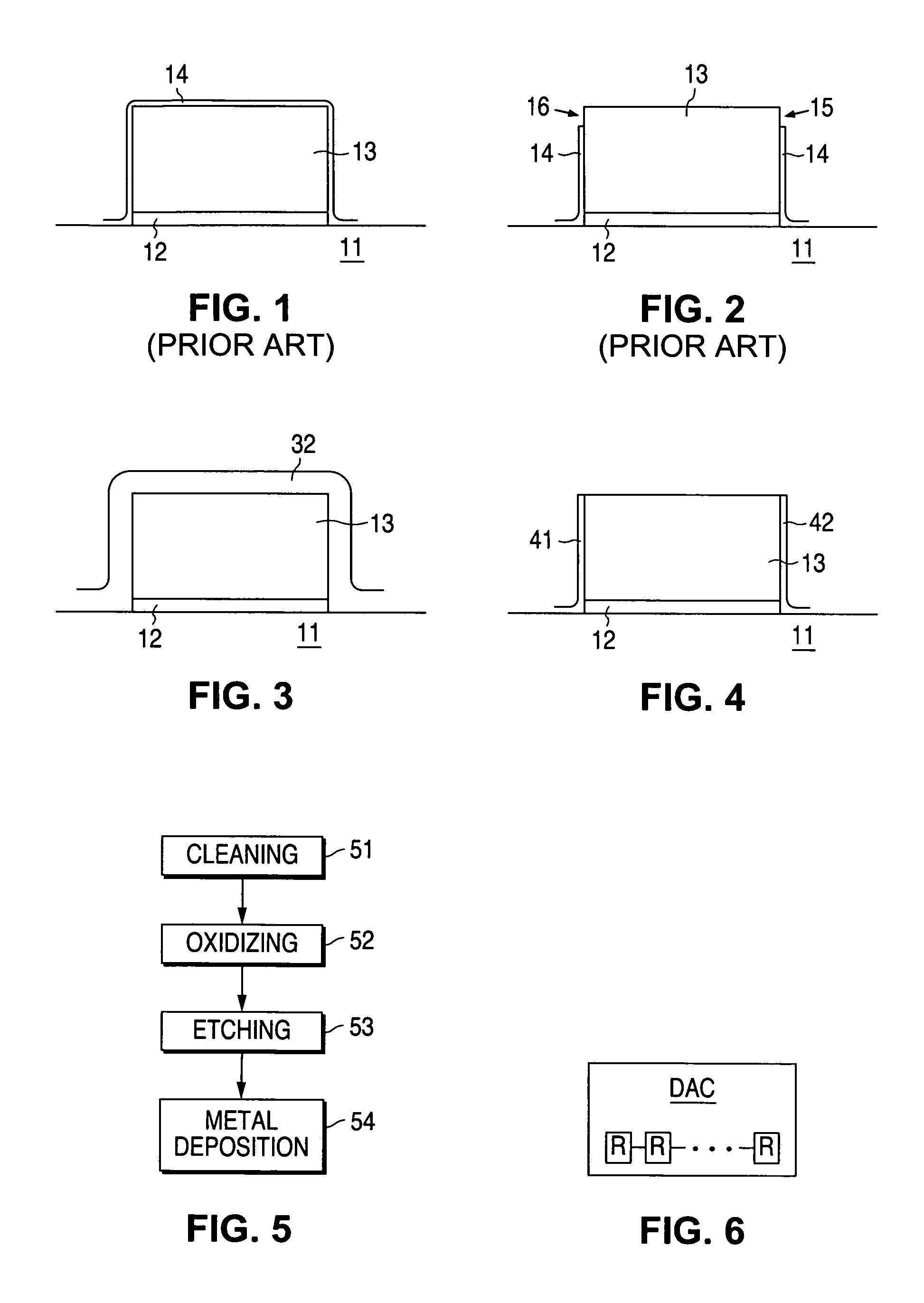
[0013]FIGS. 1 through 6, discussed below, and the various embodiments used to describe the principles of the present invention in this patent document are by way of illustration only and should not be construed in any way to limit the scope of the invention. Those skilled in the art will understand that the principles of the present invention may be implemented in any suitably arranged semiconductor manufacturing system.

[0014]FIG. 1 illustrates a semiconductor resistor structure just before pre-metal cleaning according to the prior art. The structure includes a semiconductor resistor 13, such as a doped polysilicon resistor. The resistor 13 is supported on a semiconductor substrate 11, with a suitable oxide layer 12 interposed between the resistor 13 and the substrate 11. A native is oxide layer 14 is formed on the semiconductor resistor 13. The native oxide layer 14 typically has a thickness in a range from about 10 angstroms to about 30 angstroms.

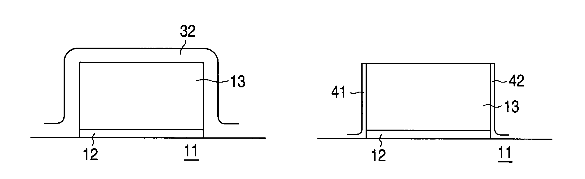
[0015]FIG. 2 illustrates the struc...


PUM


Abstract

An electrical resistance is produced in a semiconductor device by first providing a semiconductor resistor structure that includes a semiconductor resistor having formed thereon a native oxide layer. A portion of the native oxide layer that overlies a corresponding top surface portion of the semiconductor resistor is removed, in order to expose the top surface portion of the semiconductor resistor. Metal is deposited on the exposed top surface portion of the semiconductor resistor. A chemical reaction is effectuated in order to reduce the likelihood of metal reacting with the underlying silicon on any portion of the semiconductor resistor other than the top surface portion thereof. The chemical reaction can be an oxidation reaction that produces on the semiconductor resistor structure an oxide layer other than the native oxide layer and substantially thicker than the native oxide layer.

Description

TECHNICAL FIELD OF THE INVENTION[0001]The invention is directed generally to semiconductor devices and, more particularly, to manufacturing resistors in semiconductor devices.BACKGROUND OF THE INVENTION[0002]Resistors are commonly used in semiconductor devices such as integrated circuits. For example, semiconductor devices such as digital-to-analog converters or analog-to-digital converters use semiconductor resistors such as polysilicon resistors. The precision and resolution of a device such as a digital-to-analog converter is strongly dependent on the ability to match its component semiconductor resistors accurately. Mismatches as small as two percent (2%) can seriously compromise the resolution and precision of such devices.[0003]It is therefore desirable to provide for improved precision and consistency in the manufacture of semiconductor resistances.SUMMARY OF THE INVENTION[0004]Exemplary embodiments of the invention produce an electrical resistance in a semiconductor device b...

Claims


Application Information

Patent Timeline
IPC IPC(8): H01L21/8238H01L23/62
CPCH01L27/0802H01L28/20
Inventor MITRA, RESHMIRUBY, SCOTTDRIZLIKH, SERGAIFRANCIS, THOMASTRACY, ROBERT
Owner NAT SEMICON CORP
Why Eureka
Try Eureka