Multi-layered high-speed printed circuit boards comprised of stacked dielectric systems

a printed circuit board and dielectric system technology, applied in high frequency circuit adaptations, flat/ribbon cables, cables, etc., can solve the problems of increasing signal speed, increasing data rate, increasing data loss, etc., to reduce the effective dielectric constant and effective dielectric loss, and increasing the bandwidth of interconnection systems

Active Publication Date: 2010-07-13
BANPIL PHOTONICS
View PDF4 Cites 30 Cited by
  • Summary
  • Abstract
  • Description
  • Claims
  • Application Information

AI Technical Summary

Benefits of technology

[0013]Accordingly, it is an objective of the invention to provide a technique to reduce the effective dielectric constant and effective dielectric loss of the interconnection system in order to increase the bandwidth of interconnection systems for high-speed PCBs.
[0014]Accordingly, it is an objective of this invention to use an inhomogeneous dielectric system to reduce the effective dielectric loss and dielectric constant of the interconnection system.
[0015]According to the invention, it is an objective to provide an interconnection structure where a large portion of the (electromagnetic wave) is allowed to pass through air or the dielectric material, causing less dielectric loss than that of the base dielectric material on which the signal line is laid out.

Problems solved by technology

Simultaneously, achieving higher data rates and higher off-chip interconnection densities, will be increasingly difficult as IC technologies continue to evolve with increasing signal speed of electronic devices and increasing numbers of interconnections.
Technology for off-chip interconnections on PCBs is also becoming increasingly difficult with the increased density of interconnects from die-level packaging to chip-to-chip interconnections on the PCB (hereinafter “chip” indicates the die with packaging), as well as increasing signal speeds and increasing numbers of interconnections.
However, FR4 has material characteristics which limit its usage in high-speed applications with conventional interconnection structures because FR4 has a high dielectric loss which limits the bandwidth of interconnection structures.
This increased dielectric constant causes the system to experience more signal delay, increasing the need for a dielectric material with a low dielectric constant.
Such low loss tangent dielectric material is very expensive, and the manufacturing process for PCB manufacturing using these materials has not yet matured.
Additionally, PCBs made of such low loss material is not very reliable.
Implementing new material in PCB fabrication processes will be very expensive (more than ten times conventional solutions) to mature the technology.
In addition, new materials with low loss tangents will be incompatible with conventional processing using dielectric materials such as FR4, so is not a low-cost solution.
Also, existing conventional electrical interconnects have bandwidth limitations, and it would be very expensive to completely change PCB manufacturing technology to suit higher-bandwidth needs.

Method used


Image

  • Multi-layered high-speed printed circuit boards comprised of stacked dielectric systems
  • Multi-layered high-speed printed circuit boards comprised of stacked dielectric systems
  • Multi-layered high-speed printed circuit boards comprised of stacked dielectric systems

Examples


Embodiment Construction

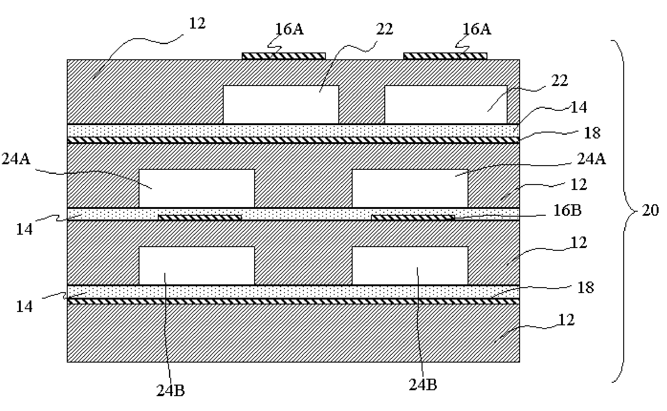
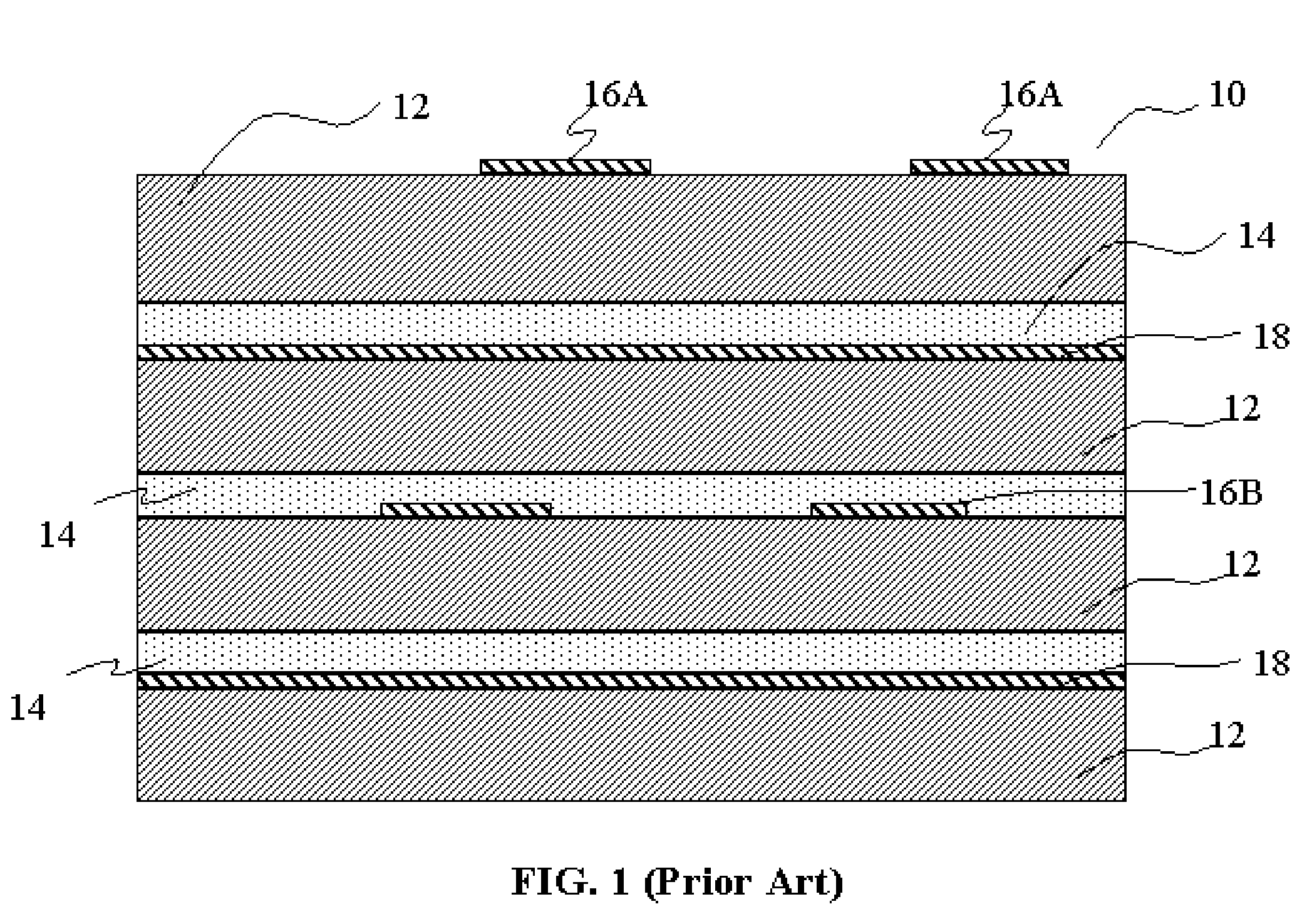
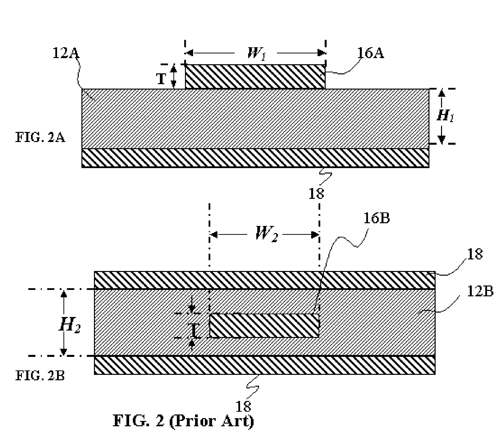
[0052]The best modes for carrying out the present invention will be described with reference to the corresponding drawings. In the following description, the same reference numerals denote components having substantially the same functions and arrangements, and duplicate explanations will be made only where necessary.

[0053]An important point of the high-speed PCB with high-speed electrical interconnects according to the present invention is that the microwave loss is to be reduced by reducing the effective loss tangent, resulting in increased bandwidth of the interconnects and an interconnection signal-speed closer to the source speed. Another important point is that the technique is to be cost-effective, and compatible with standard manufacturing technology.

[0054]In an interconnections system connecting two or more electronics elements (e.g., two or more chips), the signal can be conveyed electrically through the wire (electrical conductor) laid on the dielectric medium. For high-s...


PUM


Abstract

High speed printed circuit boards (PCBs) are disclosed comprising a dielectrics systems with the back-side trenches, prepregs, signal lines and ground-plans, wherein the signal line and ground-plan are located on the dielectrics. Using of the open trenches in the substrate help to reduce the microwave loss and dielectric constant and thus increasing the signal carrying speed of the interconnects. Thus, according to the present invention, it is possible to provide a simple high speed PCB using the conventional material and conventional PCB manufacturing which facilitates the design of circuits with controlled bandwidth based on the trench opening in the dielectrics, and affords excellent reliability. According to this present invention, high speed PCB with the interconnect system contains whole portion or portion of interconnects for high speed chips interconnects and that have have the dielectric system with opened trench or slot to reduce the microwave loss.

Description

CROSS REFERENCE TO RELATED APPLICATIONS[0001]This application claims the benefit of U.S. Provisional Patent Application No. 60 / 522,021 filed on Aug. 3, 2004.FIELD OF THE INVENTION[0002]This invention relates to high-speed electrical interconnects for chip-to-chip interconnection, more particularly on the high-speed printed circuit board (PCB), where two or more integrated circuits (ICs) are needed to connect each other's signal lines for communicating. These types of high-speed PCBs (including printed-wiring-boards (PWB)) could be used in all kinds of computers from personal computers to super-computers, servers, storage systems, game systems, imaging systems and networking systems. This invention is also related to high-speed electrical interconnections, optical interconnections, and optical-electrical interconnections, where PCBs are used for the interconnection of two or more high-speed electronics and / or optical elements.BACKGROUND OF THE INVENTION[0003]The increase of high leve...

Claims


Application Information

Patent Timeline
Patent Type & Authority Patents(United States)
IPC IPC(8): H01P3/08
CPCH01P3/084H01P3/087H01P11/003H05K1/024H01L2223/6627H01L2924/19032H05K1/0306H05K1/0313H05K3/386H05K3/4611H05K3/4614H05K3/4697
Inventor DUTTA, ACHYUT KUMAROLAH, ROBERT
Owner BANPIL PHOTONICS
Why Eureka
Try Eureka