High-speed flex printed circuit and method of manufacturing

a printed circuit and high-speed technology, applied in the direction of printed circuit, printed circuit manufacturing, high-frequency circuit adaptation, etc., can solve the problems of high-density interconnects, increasing difficulty in achieving off-chip data rates and higher interconnect densities, and high-density interconnects, so as to reduce the effective dielectric constant and effective dielectric loss, increase the bandwidth of interconnection, and reduce the effect of effective dielectric loss

Active Publication Date: 2007-03-22
BANPIL PHOTONICS
View PDF5 Cites 30 Cited by
  • Summary
  • Abstract
  • Description
  • Claims
  • Application Information

AI Technical Summary

Benefits of technology

[0013] Accordingly, it is an object of the invention to provide the technique to reduce the effective dielectric constant and effective dielectric

Problems solved by technology

Simultaneously achieving higher data rates and higher interconnects densities for off-chip, will be increasingly difficult as the IC technologies continue to evolve increasing signal speed of electronic devices and interconnection number.
In off-chip case, high density interconnects, covering from die-level packaging to chip-to-chip (hereafter chip indicates the die with package) interconnection on the FLEX-PCB, will also be getting increasingly difficult as the IC technologies continue to evolve increasing the signal speed and interconnection number.
However, Polyimide has material characteristics, which limit its usage in high speed if conventional interconnection structure is used.
The reason is that conventional Polyimide has the high dielectric loss which mainly limits the bandwidth of interconnects.
If the tangent loss of the dielectrics are high, the bandwidth of the interconnects gets so limited that, high speed signal can't be sent over longer distance as compared with the dielectrics having the lower

Method used


Image

  • High-speed flex printed circuit and method of manufacturing
  • High-speed flex printed circuit and method of manufacturing
  • High-speed flex printed circuit and method of manufacturing

Examples


Embodiment Construction

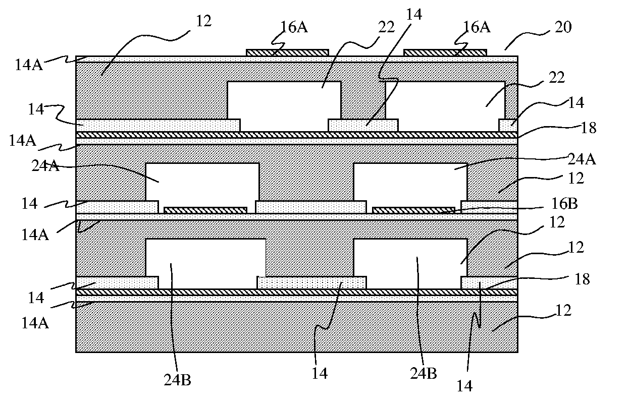
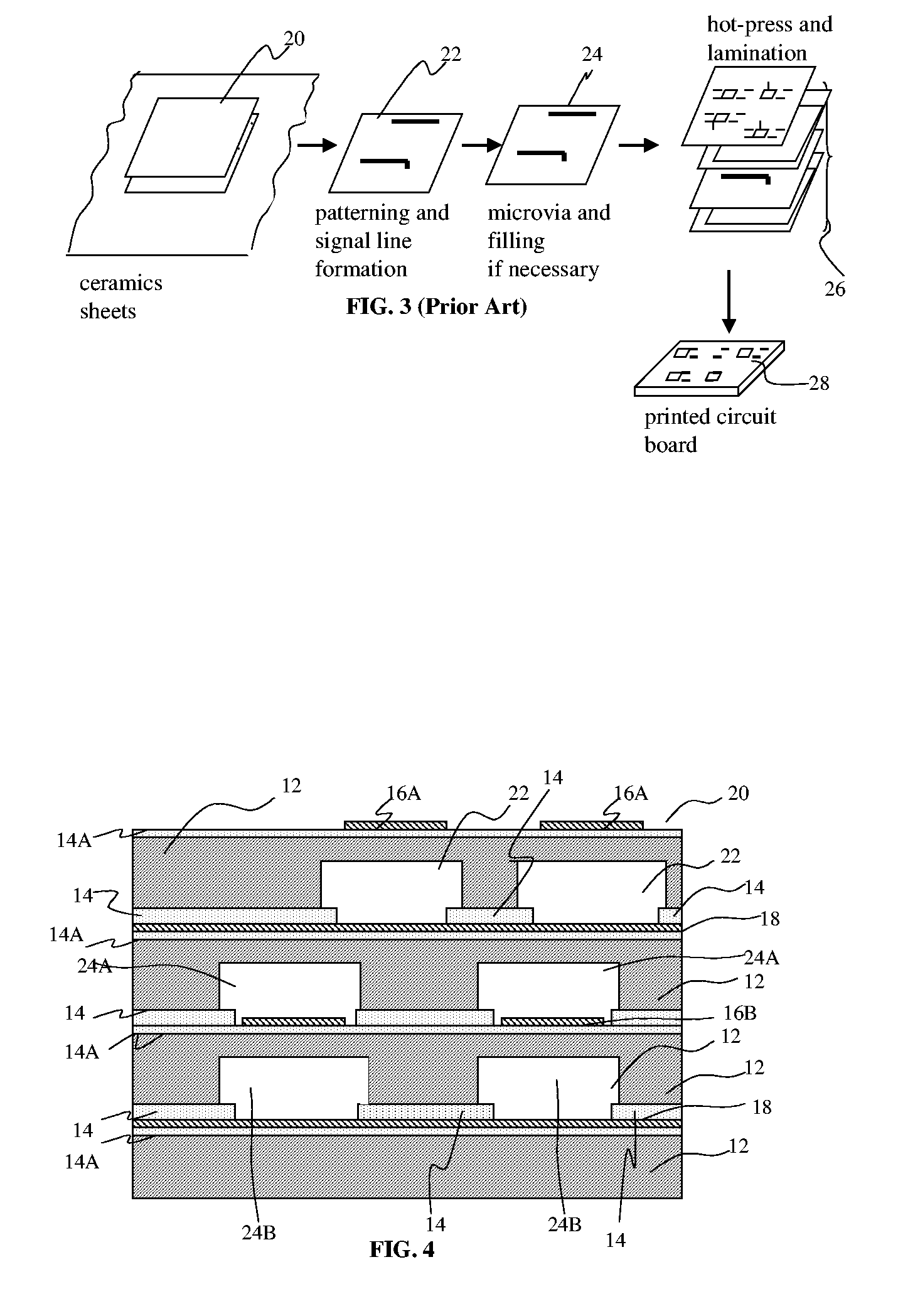
[0053] The best modes for carrying out the present invention will be described in turn with reference to the accompanying drawings. In the following description, the same reference numerals denote components having substantially the same functions and arrangements, and duplicate explanation will be made only where necessary.

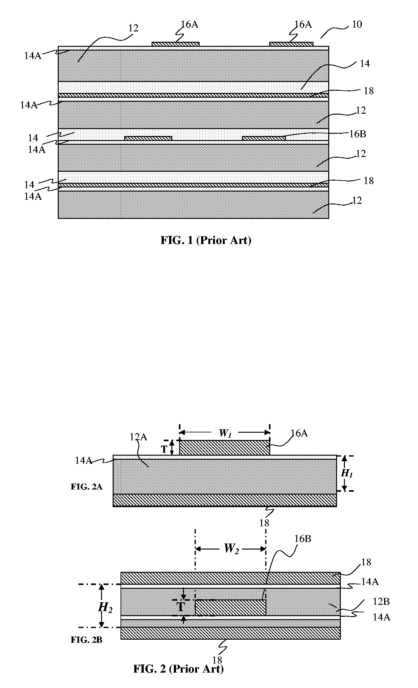
[0054] An important point of high speed FLEX-PCB having high speed electrical interconnects is that the microwave loss is to be reduced by reducing the effective dielectric constant, resulting in increasing the bandwidth of the interconnects and keeping the signal-speed of the interconnection system closer to the source speed. Other point is also kept in mind that the technique is to be cost effective, and compatible to standard manufacturing technology can be used.

[0055] In interconnects system for two or more electronics elements (two or more ICs etc.) Connections, the signal can be conveyed electrically through the wire (electrical conductor) laid on the die...


PUM

PropertyMeasurementUnit
Thicknessaaaaaaaaaa
Flow rateaaaaaaaaaa
Speedaaaaaaaaaa

Abstract

High speed flex printed circuit boards (FLEX-PCBs) are disclosed comprising a dielectrics systems with the back-side trenches, adhesives, signal lines and ground-plans, wherein the signal line and ground-plan are located on the dielectrics. Using of the open trenches in the substrate help to reduce the microwave loss and dielectric constant and thus increasing the signal carrying speed of the interconnects. Thus, according to the present invention, it is possible to provide a simply constructed high speed FLEX-PCB using the conventional material and conventional FLEX-PCB manufacturing which facilitates the design of circuits with controlled bandwidth based on the trench opening in the dielectrics, and affords excellent connection reliability. As the effective dielectric constant is reduced, the signal width is required to make wider or the dielectric thickness is required to make thinner keeping fixed characteristics impedance. The fundamental techniques disclosed here can also be used for high-speed packaging.

Description

CROSS REFERENCE TO RELATED APPLICATIONS [0001] This application claims the benefit of U.S. Provisional Patent Application No. 60 / 522,401 filed on Sep. 25, 2004.FIELD OF THE INVENTION [0002] This invention relates to high speed electrical interconnects for chip-to-chip interconnection, more particularly on the high-speed flex printed circuit board (FLEX-PCB), where two or more integrated circuits (ICs) are needed to connect each others signal lines for communicating. These types of high speed FLEX-PCBs could be in all kinds of computers covering from personnel computer to super-computer, server, storage system, game system, imaging system, and networking systems. This invention is also related to the high-speed electrical interconnection, optical interconnection or both electrical and optical interconnection where FLEX-PCB is used for two or more high-speed electronics and / or optical elements connection. BACKGROUND OF THE INVENTION [0003] The increasing of higher level of integration...

Claims


Application Information

Patent Timeline
IPC IPC(8): H01R12/24
CPCH05K1/024H05K1/0393H05K3/386H05K3/4611Y10T29/49126H05K3/4697H05K2201/09536H05K2201/09727H05K3/4635
Inventor DUTTA, ACHYUT KUMAROLAH, ROBERT
Owner BANPIL PHOTONICS
Why Eureka
Try Eureka