High speed electronics interconnect and method of manufacture

a high-speed electronics and interconnect technology, applied in the direction of waveguides, waveguide type devices, high frequency circuit adaptations, etc., can solve the problems of increasing the difficulty of interconnecting electronic devices increasing the difficulty of high-density interconnects, and increasing the difficulty of interconnecting electronic devices. without sacrificing signal speed, to achieve the effect of reducing the effective dielectric constant and effective dielectric constant, increasing the bandwidth of interconnection

Active Publication Date: 2008-05-13
BANPIL PHOTONICS
View PDF13 Cites 8 Cited by
  • Summary
  • Abstract
  • Description
  • Claims
  • Application Information

AI Technical Summary

Benefits of technology

[0025]Accordingly, it is an object of the invention to provide the technique to reduce the effective dielectric constant and effec...

Problems solved by technology

Simultaneously achieving higher data rates and higher interconnect densities for both on-chip and also off-chip, will be increasingly difficult as the IC technologies continue to evolve increasing signal speed of electronic devices and interconnection number.
In on-chip cases (intra chip), as the number of the electronic devices such as transistor are increasing with development of the fabrication technology, the interconnecting the electronic devices without sacrificing the signal speed is getting challenging.
In off-chip case, high density interconnects, covering from die-level packaging to chip-to-chip (hereafter chip indicates the die with package) interconnection on the printed circuit board (PCB), will also be getting increasingly difficult as the IC technologies continue to evolve increasing the signal speed and interconnection number.
Impedance mismatch must be minimized to reduce the reflections and prevent ringing, which can cause false decision (switching) in the receiver signal.
Significant attenuation and rise-time de...

Method used


Image

  • High speed electronics interconnect and method of manufacture
  • High speed electronics interconnect and method of manufacture
  • High speed electronics interconnect and method of manufacture

Examples


first embodiment

[0073]An important point of high speed electronic interconnects system is that the microwave loss is to be reduced by reducing the effective dielectric constant, resulting in increasing the bandwidth of the interconnects and keeping the signal-speed of the interconnection system closer to the source speed. Other point is also kept into mind that the technique is to be cost effective, and compatible to standard manufacturing technology can be used.

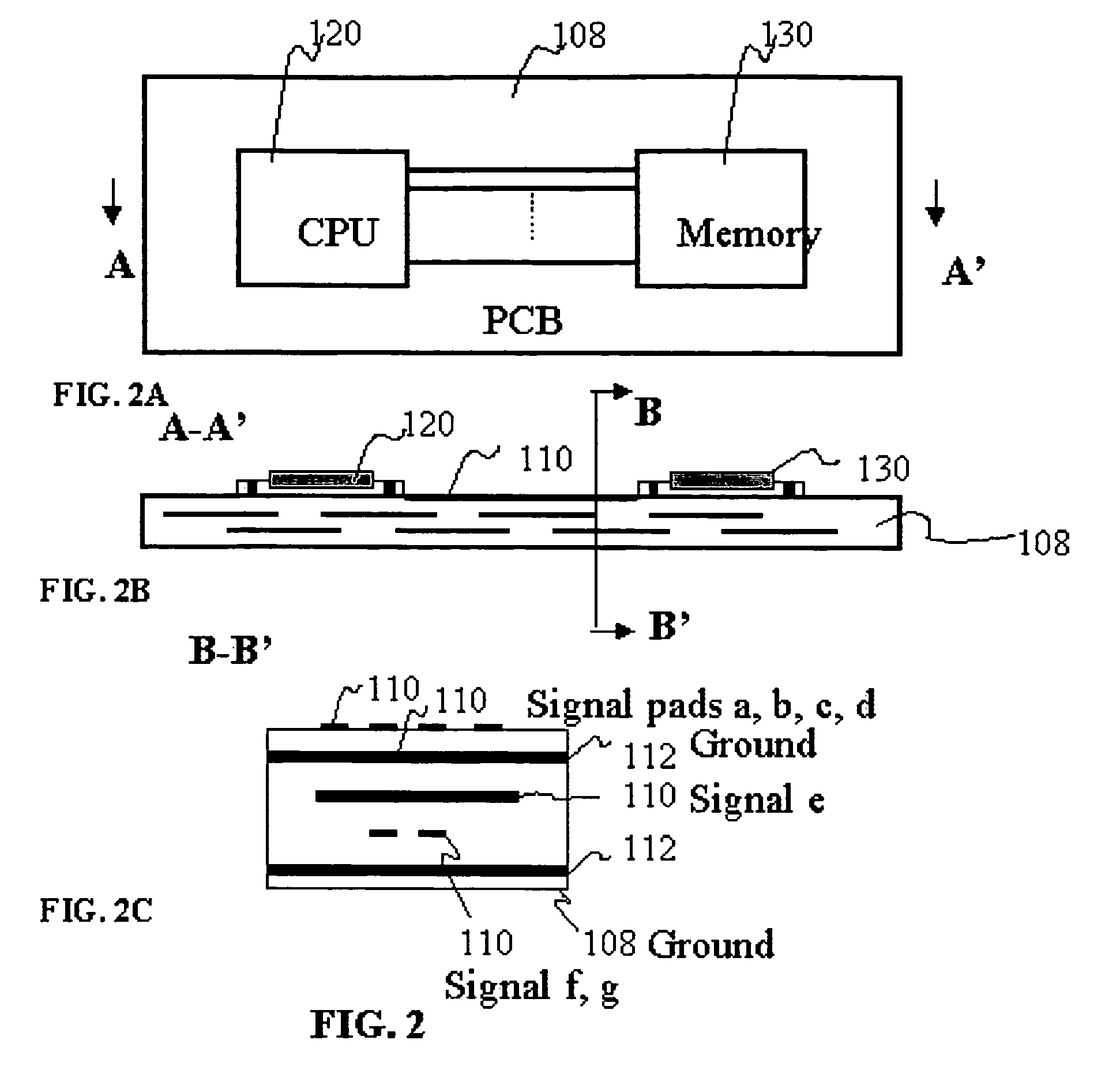
[0074]In interconnects system for two or more electronics elements (on-chip electronic devices such as transistors, or two or more ICs etc.) connections, the signal can be conveyed electrically through the wire (electrical conductor) laid on the dielectric medium. For high speed signal transmission electrical conductor is to be transmission line of type microstrip or strip line. The signal speed in the interconnects (i.e. bandwidth of the interconnects system) is mainly dominated by; (a) signal conductor parameters (i) length and (ii) thic...

third embodiment

[0080]FIG. 10 comparing the frequency responses of microstrip configurations shown in FIG. 6 and FIG. 8, as the prior art and the preferred embodiment in the third embodiment according to the invention. Due to reduction of the microwave-loss, the frequency response can be improved tremendously as compared with the conventional mircrostrip line where the electrical field is uniformly distributed away from the signal line.

[0081]According to the invention, based on the interconnect structure design, the effective dielectric loss and effective dielectric constant of the interconnect system can be controlled. This helps to add many features in the interconnection such as varying the phase velocity (which is function of the dielectric constant), varying the bandwidth of the interconnect; help to adjust the skews of the signal etc. in the single interconnect system. According to the preferred embodiment, ideally, the speed of the signal in the signal line can be made to speed of the light ...

fifth embodiment

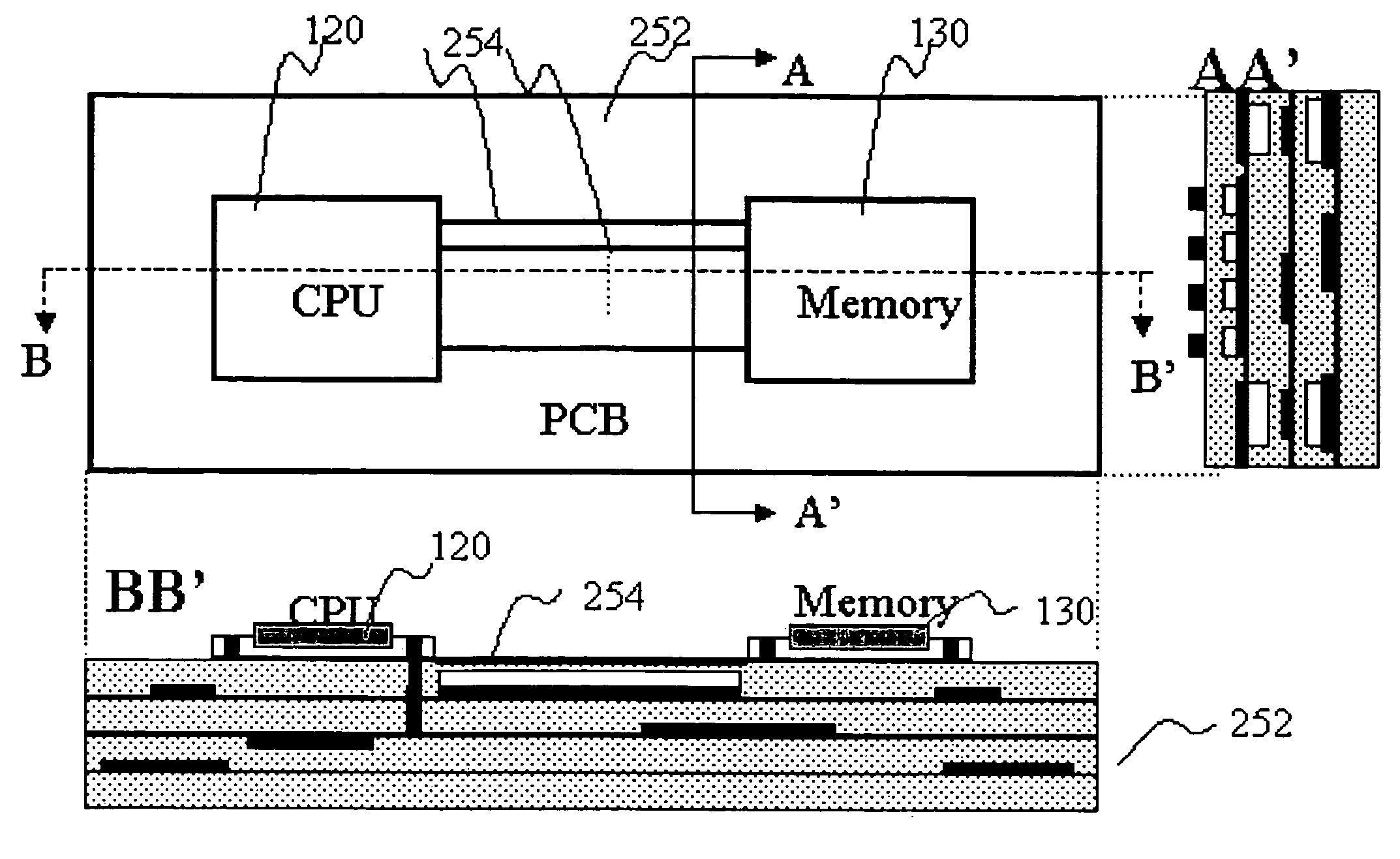
[0093]FIG. 12 shows the flow-chart of the printed circuit board fabrication process for the off-chip interconnects in the fifth embodiment in accordance to the invention, where in the like parts are indicated by the like numerals, so that repeated explanation is omitted here. The dielectric sheet (not shown) is made using the standard PCB technology for example using the slurry casting process. The slurry is cast into about 200 μm to 500 μm thick ceramic sheets by slip cast process. The PCB core layer 244 is the conventional PCB layer. Metallization sheet 246 is made using the conventional PCB technology. After the metallization, the trench or slot is opened in sheet 248 by using the processes such as laser drilling, or dry-etching or wet-etching (following patterning for etching) or mechanical drilling. Via holes are formed through the dielectric sheet with air holes 244 by a punching machine with punches and dies. A ceramic sheet 244 may have more than 10,000 via holes in a 250 mm...


PUM


Abstract

Fundamental interconnect systems for connecting high-speed electronics elements are provided. Interconnect system has the means, which could reduce the microwave loss by reducing the effective dielectric loss and dielectric constant of the interconnect system, and increase the bandwidth of the interconnects and also reduce the signal propagation delay, respectively. Ideally, the speed of the electrical signal on the signal line can be reached to speed of the light in the air, and the bandwidth can be reached to closer to the optical fiber. The interconnect systems consists of the signal line, dielectric system with opened trench or slot filled up with the air or lower dielectric loss material, and the ground plan. The signal line proposed in this invention could be made any type of signal line configuration for example, microstripline, strip line or coplanar line. The signal line can also be made as single ended or differential pairs of any configurations. The interconnect system based on the fundamental techniques provided in this invention, can be used for on-chip interconnects where the high speed electronics devices are connected by the signal line laid on the oxide or dielectric material. Again, the interconnect system based on the fundamental techniques provided in this invention, can also be used for off-chip interconnects (chip-to-chip interconnects), where the whole portion or portion of the PCB on which high speed chips are to be connected, are having the dielectric system with opened trench or slot to reduce the microwave loss. High scale chip-to-chip interconnection using of the multilayered PCB is possible. The fundamental techniques provided in this invention can also be used for high-speed connectors and high-speed cables. The main advantages of this invention are to make high speed interconnects systems for on-chip and off-chip interconnects. More over, this fundamental technology is also used for the high sped die package, high speed connector, and high speed cables where conventional manufacturing technology can be used and yet to increase the bandwidth of the interconnects.

Description

CROSS REFERENCE TO RELATED APPLICATIONS[0001]This application claims the benefit of U.S. Provisional Application No. 60 / 451,950 filed Mar. 5, 2003.FIELD OF THE INVENTION[0002]This invention relates to interconnection of electronics elements in on-chip (intra-chip) and off-chip (inter chip) level interconnection, high-speed connector, cable fabrication, and also high speed packaging. More particularly, this invention is related to, (a) connecting two or more electronic devices inside the chip (for intrachip connection), (b) connecting the high speed signal line of single or multi processor chips to signal line of single or multi memory chips, which are used in all kinds of computers covering from personnel computer to super-computer, server, storage system, and also in game system, (c) also interface means (as the connector or cable) to connect two or multiple high speed electronics elements, and (d) also high speed packaging to connect the chip to package. This invention is also rel...

Claims


Application Information

Patent Timeline
IPC IPC(8): H01L21/00H01L23/538H01L23/66H01L25/065H05K1/00H05K1/02H05K1/03
CPCH01L23/5383H01L23/66H01L25/0655H01P1/2005H01P3/08H05K1/0236H05K1/024H05K1/0253H01L2924/13091H01L2224/48091H01L2224/16225H01L2223/6627H01L2924/09701H01L2924/12044H01L2924/1903H01L2924/19032H01L2924/19033H01L2924/3011H05K1/0224H05K1/0298H05K1/0306H05K1/0313H05K2201/0187H05K2201/0191H05K2201/0715H05K2201/09036H05K2201/09063H05K2201/09681H01L2924/00014H01L2924/00H01L2224/05573H01L2224/05568Y02P80/30H01L2224/05599
Inventor DUTTA, ACHYUT
Owner BANPIL PHOTONICS
Why Eureka
Try Eureka