High-Speed Printed Circuit Boards (PCBs) and Manufacturing

a printed circuit board and high-speed technology, applied in the direction of waveguides, high-frequency circuit adaptations, waveguide type devices, etc., can solve the problems of increasing the difficulty of high-density interconnects, so as to reduce the effective dielectric constant and effective dielectric loss, increase the bandwidth of interconnections, the effect of increasing the bandwidth

Active Publication Date: 2006-02-09
BANPIL PHOTONICS
View PDF4 Cites 74 Cited by
  • Summary
  • Abstract
  • Description
  • Claims
  • Application Information

AI Technical Summary

Benefits of technology

[0013] Accordingly, it is an object of the invention to provide the technique to reduce the effective dielectric constant and effective dielectric loss of interconnection system especially dielectric material, to increase the bandwidth of the interconnection for building high speed PCB.

Problems solved by technology

Simultaneously achieving higher data rates and higher interconnects densities for off-chip, will be increasingly difficult as the IC technologies continue to evolve increasing signal speed of electronic devices and interconnection number.
In off-chip case, high density interconnects, covering from die-level packaging to chip-to-chip (hereafter chip indicates the die with package) interconnection on the PCB, will also be getting increasingly difficult as the IC technologies continue to evolve increasing the signal speed and interconnection number.
However, FR4 has material characteristics, which limit its usage in high speed if conventional interconnection structure is used.
The reason is that conventional FR4 has the high dielectric loss which mainly limit the bandwidth of the interconnects.
If the tangent loss of the dielectrics are high, the bandwidth of the interconnects gets so limited that, high speed signal can't be sent over longer distance as compared with the dielectrics having the lower tangent loss.
These causes signal skews for the different length of signal lines.
This dielectric material is very high cost and the manufacturing process for building PCB using these materials are not matured yet.
In addition, the PCB made of such low loss material has low reliability.
Implementing new material in PCB fabrication process will cost tremendously high (more than ten times over conventional solution) to make it mature.
In addition, new materials having low tangent loss is a material incompatible with conventional dielectric material such as FR4 processing, so is not a low cost solution.
In both cases, implementing technology would need to pay high cost.
As explained above, the conventional PCB technology being used for off-chip interconnection couldn't be used as the need of the signal speed is increasing.
And also existing conventional electrical interconnects have the limitation of achieving the bandwidth in certain level, beyond that complete manufacturing technology is needed to be changed which is costly for PCB industries.

Method used


Image

  • High-Speed Printed Circuit Boards (PCBs) and Manufacturing
  • High-Speed Printed Circuit Boards (PCBs) and Manufacturing
  • High-Speed Printed Circuit Boards (PCBs) and Manufacturing

Examples


first embodiment

[0053] An important point of high speed PCB having high speed electrical interconnects is that the microwave loss is to be reduced by reducing the effective tangent loss, resulting in increasing the bandwidth of the interconnects and keeping the signal-speed of the interconnection system closer to the source speed. Other point is also kept in mind that the technique is to be cost effective, and compatible to standard manufacturing technology can be used.

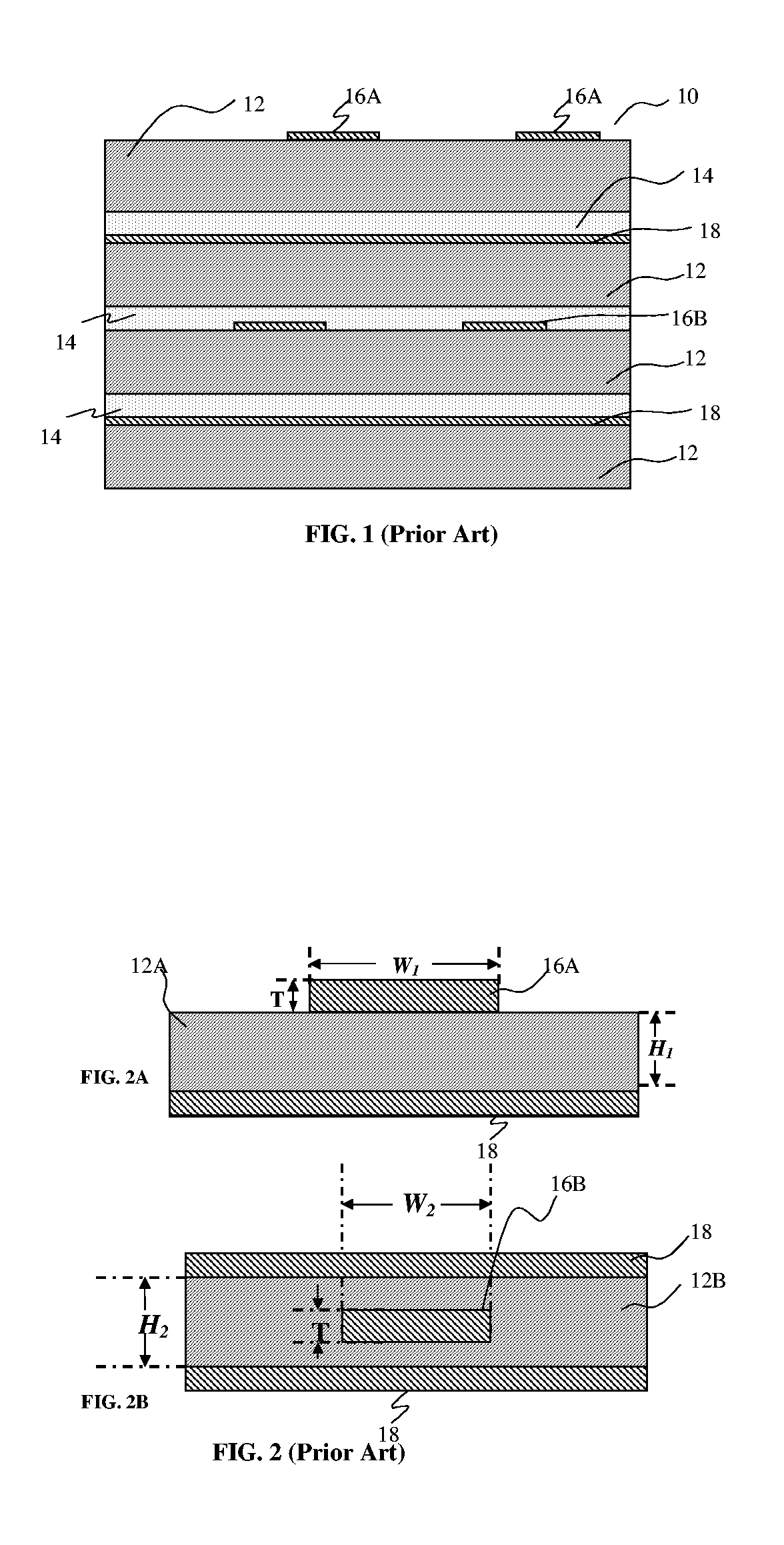
[0054] In interconnects system for two or more electronics elements (two or more chips etc.) Connections, the signal can be conveyed electrically through the wire (electrical conductor) laid on the dielectric medium. For high speed signal transmission electrical conductor is to be transmission line of type microstrip or strip line. The signal speed in the interconnects (i.e. bandwidth of the interconnects system) is mainly dominated by; (a) signal conductor parameters (i) length and (ii) thickness, and (b) dielectric material proper...

fifth embodiment

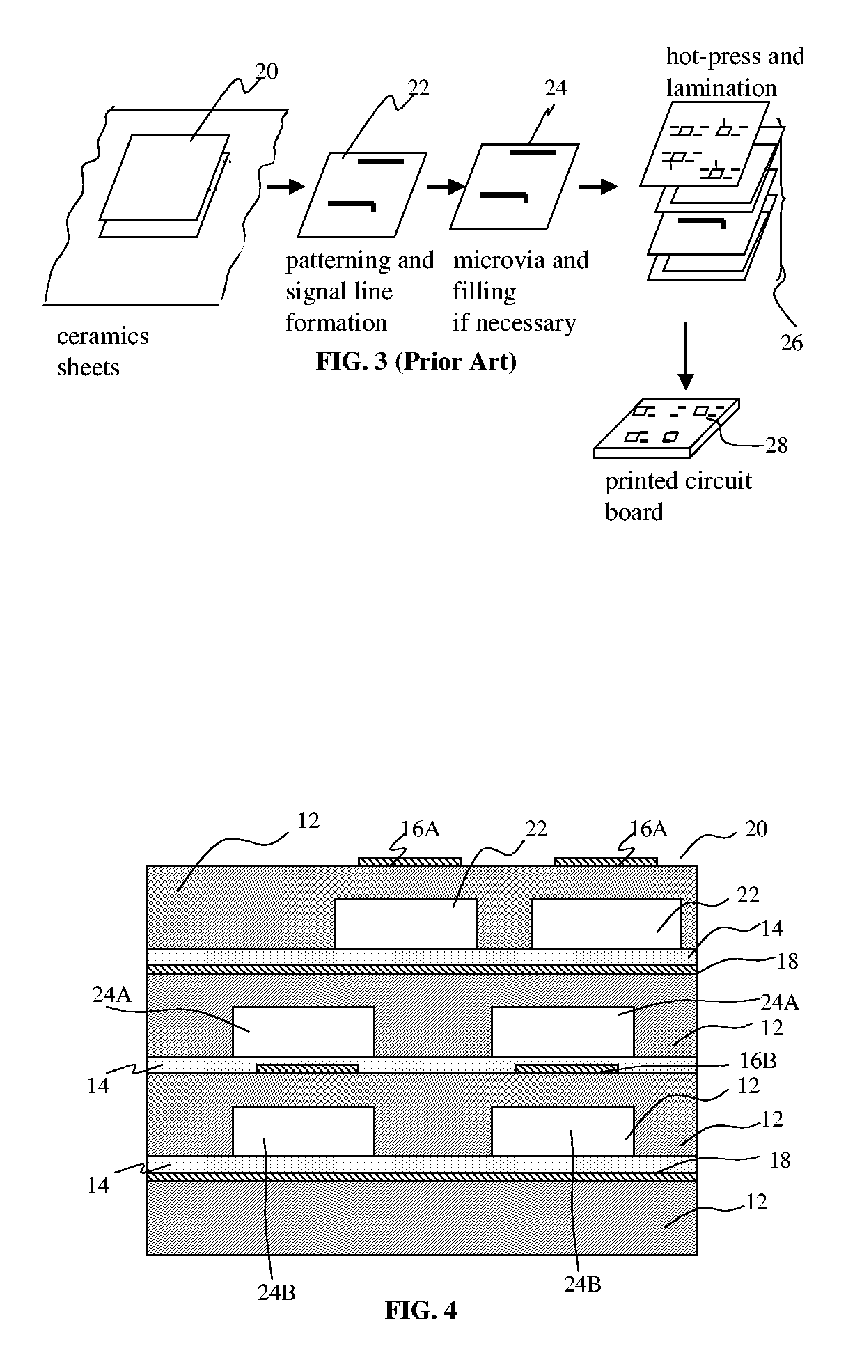
[0077]FIG. 8 shows the flow-chart of the high speed mulitlayered PCB fabrication process for the off-chip interconnects in the fifth embodiment in accordance to the invention, where in the like parts are indicated by the like numerals, so that repeated explanation is omitted here. The dielectric sheet (not shown) is made using the standard PCB technology for example using the slurry casting process. The slurry is cast into about 200 μm to 500 μm thick ceramic sheets by slip cast process. Each dielectrics sheet material 44 is the conventional PCB core layer 44. Metallization sheet 46 is made using the conventional PCB technology. After the metallization, the trench or slot is opened in sheet 48 by using the processes such as laser drilling, or dry-etching or wet-etching (following patterning for etching) or mechanical drilling. Via holes are formed through the dielectric sheet 44 by a punching machine with punches and dies. A ceramic sheet 44 may have more than 10,000 via holes in a ...

seventh embodiment

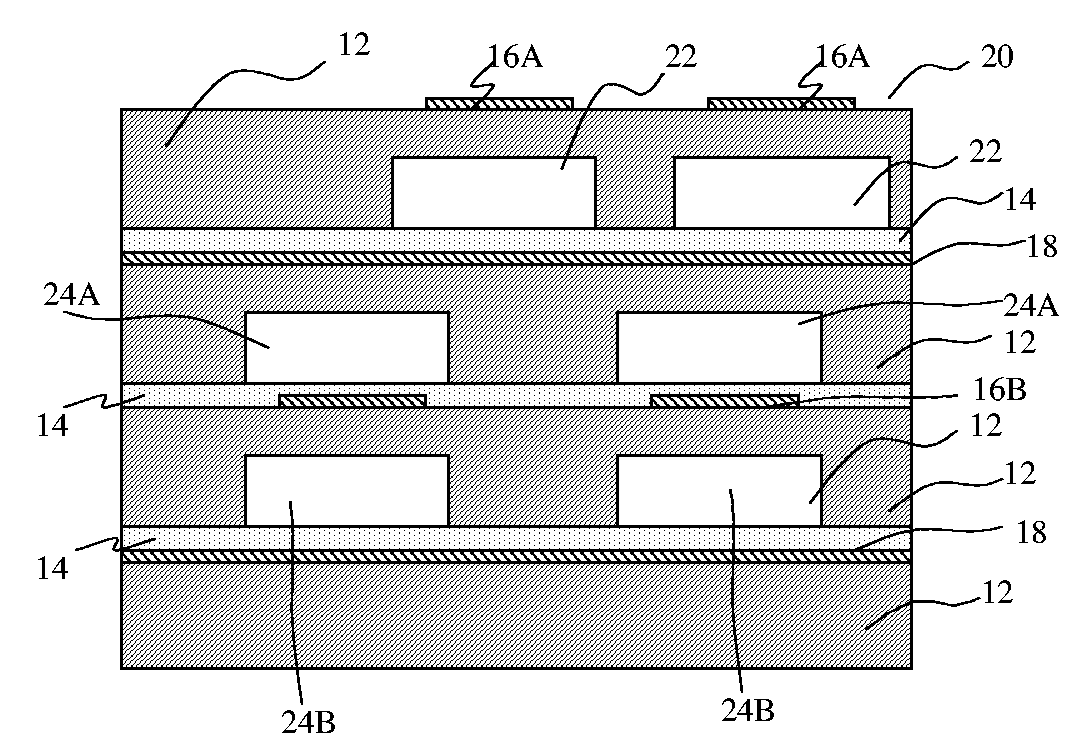
[0080]FIGS. 10A and 10B show the schematic showing the enlarged top views of the signal line layout which is connecting to the via or microvia in the case of multi-layered high speed PCB with the high speed signal lines and micro-via embedded into the PCB, in the seventh embodiment in accordance to the invention, where in the like parts are indicated by the like numerals, so that repeated explanation is omitted here. According to this invention, signal lines consisting of signal lines 58 and 60 (located on the surface 62) may have / haven't have transition. The transition of the signal lines 58 with underneath air-cavities (opened trenches) 24 (24A and 24B) to the signal lines 60 without air-cavities (opened trenches) prior to the via 54. For smooth transition without reflection of the signal, the transition length l3 is used. The shape of the transition could be trapezoidal or circular or ellipsoidal (not shown).


PUM


Abstract

High speed printed circuit boards (PCBs) are disclosed comprising a dielectrics systems with the back-side trenches, prepregs, signal lines and ground-plans, wherein the signal line and ground-plan are located on the dielectrics. Using of the open trenches in the substrate help to reduce the microwave loss and dielectric constant and thus increasing the signal carrying speed of the interconnects. Thus, according to the present invention, it is possible to provide a simple high speed PCB using the conventional material and conventional PCB manufacturing which facilitates the design of circuits with controlled bandwidth based on the trench opening in the dielectrics, and affords excellent reliability. According to this present invention, high speed PCB with the interconnect system contains whole portion or portion of interconnects for high speed chips interconnects and that have have the dielectric system with opened trench or slot to reduce the microwave loss.

Description

CROSS REFERENCE TO RELATED APPLICATIONS [0001] This application claims the benefit of U.S. Provisional Patent Application No. 60 / 522,021 filed on Aug. 3, 2004.FIELD OF INVENTION [0002] This invention relates to high speed electrical interconnects for chip-to-chip interconnection, more particularly on the high-speed printed circuit board (PCB), where two or more integrated circuits (ICs) are needed to connect each other's signal lines for communicating. These types of high speed PCBs (also covering printed-wiring-board (PWB)) could be used in all kinds of computers covering from personnel computer to super-computer, server, storage system, game system, imaging system and networking systems. This invention is also related to the high-speed electrical interconnection, optical interconnection or both electrical and optical interconnection where PCB is used for two or more high-speed electronics and / or optical elements connection. BACKGROUND OF INVENTION [0003] The increasing of higher l...

Claims


Application Information

Patent Timeline
Patent Type & Authority Applications(United States)
IPC IPC(8): H01P3/08
CPCH01L2223/6627H01L2924/19032H01P3/084H01P3/087H01P11/003H05K3/4697H05K1/0306H05K1/0313H05K3/386H05K3/4611H05K3/4614H05K1/024
Inventor DUTTA, ACHYUT KUMAROLAH, ROBERT
Owner BANPIL PHOTONICS
Why Eureka
Try Eureka