Optical element, liquid crystal device, and display

a liquid crystal device and optical element technology, applied in the direction of instruments, polarizing elements, projectors, etc., can solve the problems of reducing display quality or the like, destabilizing the operation of the liquid crystal panel, and undesirable reflected light generated on the optical path, so as to inhibit suppress the negative influence of reflected light

Active Publication Date: 2010-07-13
SEIKO EPSON CORP
View PDF4 Cites 35 Cited by
  • Summary
  • Abstract
  • Description
  • Claims
  • Application Information

AI Technical Summary

Benefits of technology

[0008]An advantage of the present invention is to provide an optical element that enables suppression of negative influence of reflected light.
[0009]Another advantage of the invention is to provide a high-performance liquid crystal device including the above optical element.
[0010]Still another advantage of the invention is to provide a high-performance display including the above optical device.
[0011]An optical element according to a first aspect of the invention has a function of splitting incident light into polarized beams. The optical element includes a substrate transparent for the incident light; a diffractive structure that includes a plurality of concave portions and a plurality of convex portions alternately arranged with each other, each of the plurality of concave portions and convex portions having a rectangular sectional shape, and that is provided on a first surface of the substrate; and a grid that includes a plurality of fine lines extending in a single direction and that is provided along a top surface of the diffractive structure on the first surface of the substrate, wherein the conditions: d<λ and λ / n<δ≦λ are satisfied when λ represents a wavelength of the incident light; d represents a distance between the neighboring fine lines; δ represents a distance between the neighboring convex portions; and n represents a refractive index of a material forming the substrate.
[0012]In the optical element according to the first aspect, one of polarized components of the incident light is reflected by the grid, whereas the other one of the polarized components is transmitted. The reflected polarized component (the reflected light) is diffracted at a sufficiently large angle by the diffractive structure. Satisfying the relationships among the foregoing parameters allows the diffracted reflected light to be totally reflected at an interface between a second surface of the substrate and a medium surrounding the substrate (such as air). Then, the reflected diffraction light is guided through an inside of the substrate and reach the sides of the substrate. Accordingly, when the optical element of the first aspect is used in a desired optical system, almost all of light reflected by the grid do not return to a preceding stage side on an optical path, thereby inhibiting negative influence of unnecessary reflected light.
[0013]Preferably, in the optical device of the first aspect, a height gap between the concave portions and the convex portions of the diffractive structure is set to a value of (2m+1)λ / 4n, where m is an integer, 0 or over. In this case, as mentioned above, λ represents the wavelength of the incident light and n represents the refractive index of the material of the substrate.

Problems solved by technology

Accordingly, there is a concern that the reflected light (the TE-polarized component) returns to the liquid crystal panel, thereby destabilizing operation of the liquid crystal panel.
In any of those optical devices, unnecessary reflected light generated on an optical path is undesirable.
Specifically, for example, when a thin film transistor is included in the liquid crystal light valve, entry of unnecessary light is likely to cause a malfunction of the thin film transistor, thereby resulting in reduction of display quality or the like.

Method used


Image

  • Optical element, liquid crystal device, and display
  • Optical element, liquid crystal device, and display
  • Optical element, liquid crystal device, and display

Examples


first embodiment

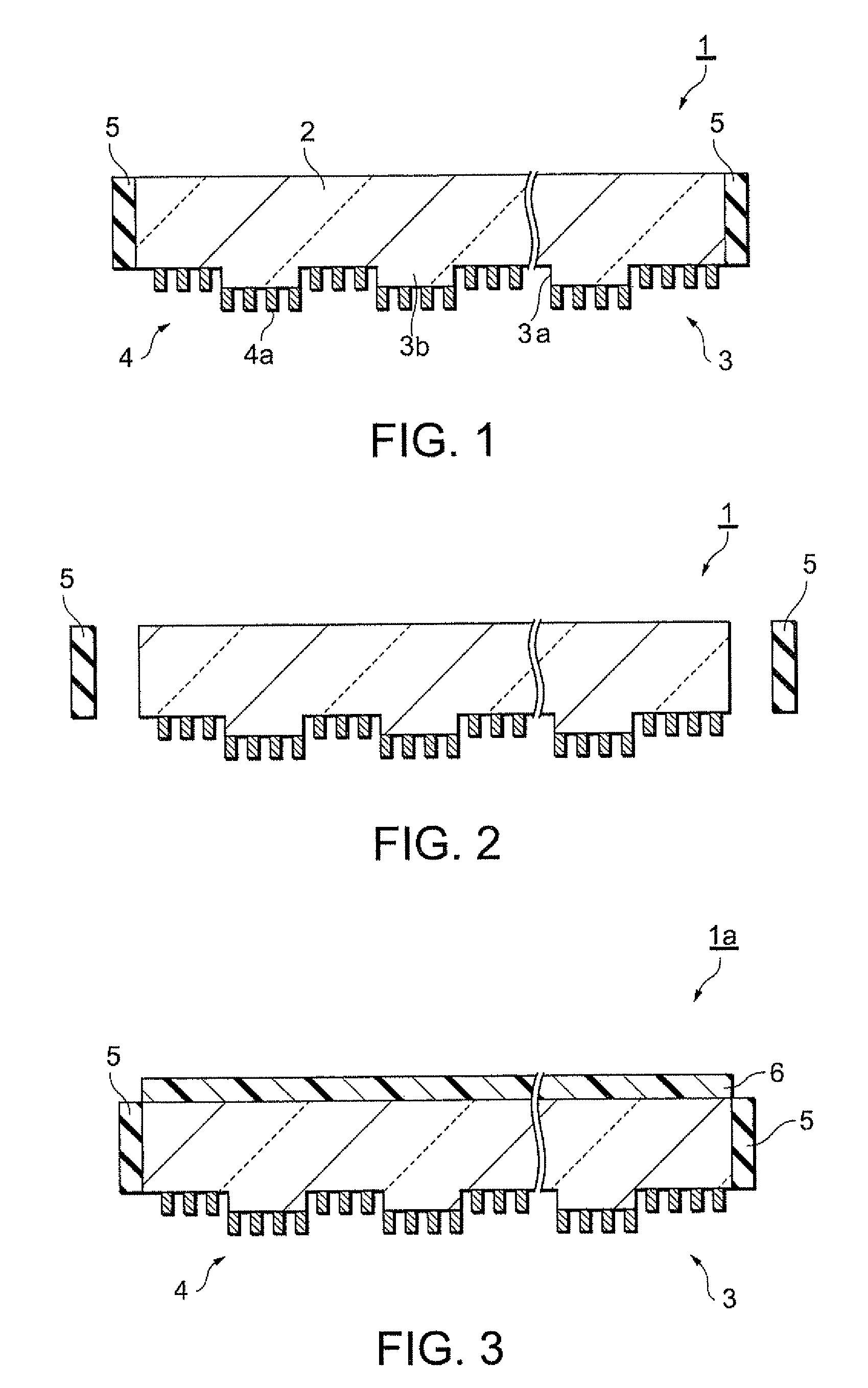
[0061]FIG. 3 is a schematic sectional view illustrating an optical element according to a modification of the An optical element 1a shown in FIG. 3 has the same structure as that of the optical element 1 in FIG. 1, and further includes an anti-reflective film 6. For example, the anti-reflective film 6 is a multilayered dielectric film. Constituent elements other than the anti-reflective film 6 are given the same reference numerals as those in the optical element 1 in FIG. 1 and descriptions thereof are omitted. Including the anti-reflective film 6 reduces light reflection at the second surface of the substrate 2.

third embodiment

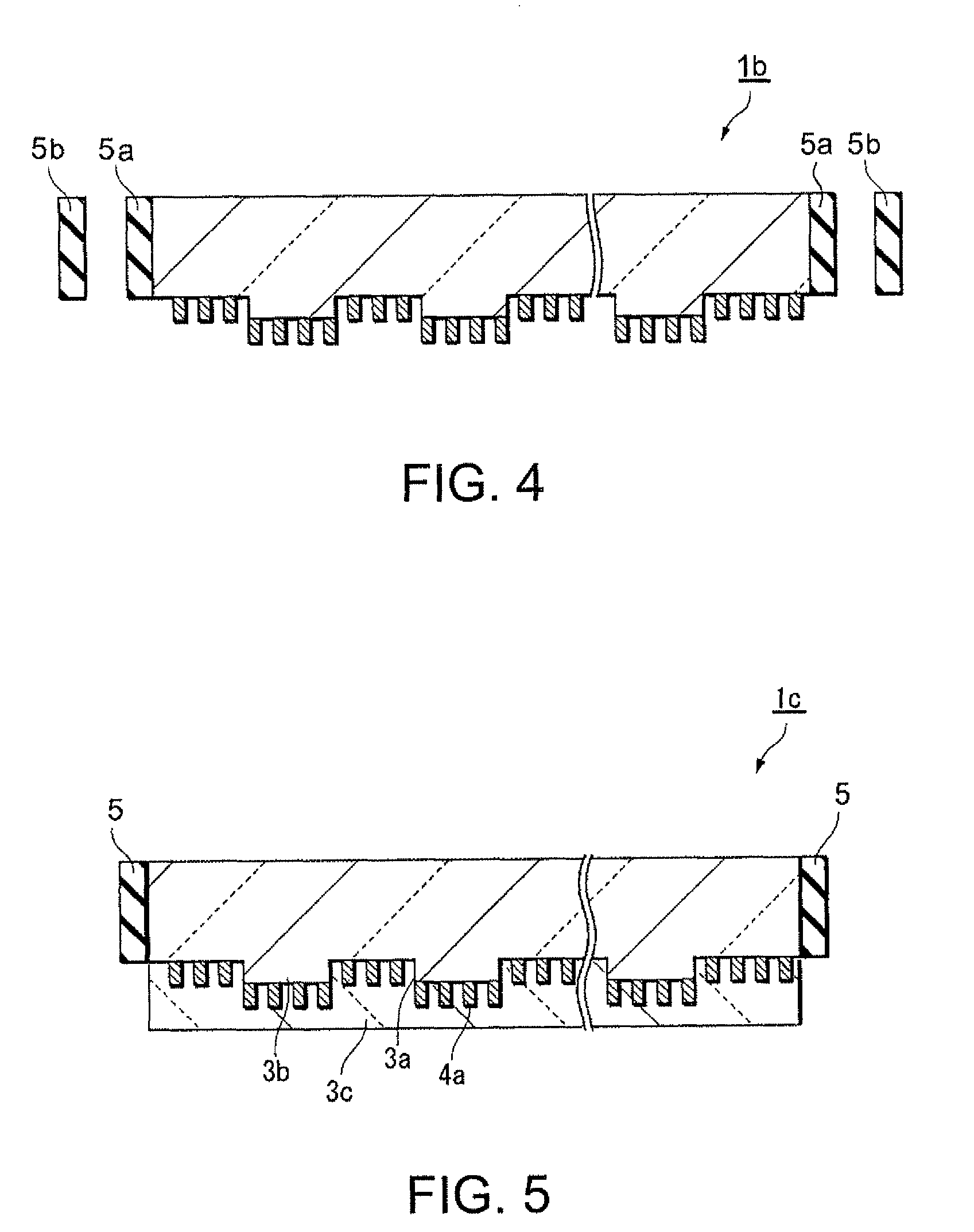
[0062]FIG. 4 is a schematic sectional view illustrating an optical element according to the invention. An optical element 1b shown in FIG. 4 has the same structure as that of the optical element 1 in FIG. 1, and further includes an anti-reflective film such as an anti-reflective coating film (an AR film). The anti-reflective film is provided as a light-attenuating portion 5a at each end of the substrate 2. Additionally, the optical element 1 further includes a light absorbing member 5b that absorbs light passing through the light-attenuating portion 5a. Providing the above-said anti-reflective film allows light reflectance to be significantly reduced at the interface between the each end of the substrate 2 and air. Thereby, the intensity of light reflected at the interface therebetween is attenuated as compared with that before reflection. This significantly reduces re-incidence of the light reflected back at the interface of the each end to the grid 4. Additionally, the light passi...

fourth embodiment

[0063]FIG. 5 is a schematic sectional view of an optical element according to the invention. An optical element 1c shown in FIG. 5 has the same structure as that of the optical element 1 in FIG. 1, and further includes a coverage film 3c provided on a side of the substrate 2 having the diffractive structure 3 formed thereon. The coverage film 3c fills the height gap between the concave and the convex portions 3a and 3b and is arranged so as to cover the concave and the convex portions 3a, 3b and the fine lines 4a. The flattening film 3c is formed by depositing a film of spin-on-glass (SOG), polysilazane, or the like, by using a liquid phase process such as a coating process. The coverage film 3c has a refractive index approximately equal to that of the substrate 2, so that light transmitting through the optical element 1b is not influenced by the height gap between the concave and the convex portions 3a and 3b. Thereby, the light transmitting through the optical element 1b is hardly...


PUM

PropertyMeasurementUnit
height gapaaaaaaaaaa
intersection angleaaaaaaaaaa

Abstract

An optical element having a function of splitting incident light into polarized beams includes a substrate transparent for the incident light; a diffractive structure that includes a plurality of concave portions and a plurality of convex portions alternately arranged with each other, each of the plurality of concave portions and convex portions having a rectangular sectional shape and that is provided on a first surface of the substrate; and a grid that includes a plurality of fine lines extending in a single direction and that is provided across a top surface of the diffractive structure on the first surface of the substrate, wherein conditions: d<λ and λ / n<δ≦λ are satisfied when λ represents a wavelength of the incident light; d represents a distance between the neighboring fine lines; δ represents a distance between the convex portions; and n represents a refractive index of a material forming the substrate.

Description

[0001]The entire disclosure of Japanese Patent Application No. 2007-210244, filed Aug. 10, 2007, is expressly incorporated by reference herein.BACKGROUND[0002]1. Technical Field[0003]The present invention relates to an optical element having a polarizing beam-splitting function, as well as to a liquid crystal device and a display each using the optical element,[0004]2. Related Art[0005]Among optical elements having a polarized beam splitting function, there is known a polarized beam splitting element of a wire grid type. The wire-grid polarized-beam splitting element includes a large number of fine wires (such as fine lines made of aluminum) arranged on a surface of a glass substrate or the like. The wires are spaced apart from each other by a distance (a cycle) shorter than a wavelength of light. The wire-grid polarized-beam splitting element is characterized by excellent polarized-beam splitting capability, as well as high optical-damage threshold because of an inorganic material ...

Claims


Application Information

Patent Timeline
Patent Type & Authority Patents(United States)
IPC IPC(8): G02F1/1335G02B27/28G02B5/30
CPCG02B5/1809G02F1/133528G02F2001/133548G02F1/133548
Inventor AMAKO, JUNSAWAKI, DAISUKE
Owner SEIKO EPSON CORP
Why Eureka
Try Eureka