Flexible circuit board connector

a flexible circuit board and connector technology, applied in the direction of coupling contact members, fixed connections, coupling device connections, etc., can solve the problems of 4 mm, difficult to realize the narrow pitch, and the low density of conductors, and achieve the effect of easy matching of characteristic impedances, increasing folding force, and high speed

Inactive Publication Date: 2010-08-03
DDK LTD
View PDF18 Cites 55 Cited by
  • Summary
  • Abstract
  • Description
  • Claims
  • Application Information

AI Technical Summary

Benefits of technology

[0037]The connector device 1 is so constructed that when said pushing portions 36 of said pivoting member 16 are pivotally moved between said pressure receiving portions 20 and connection portions 24 of said contacts 15 and said ground members 17 or between said pressure receiving portions 20 and said housing 12, rotational axes 50 of said pushing portions 36 progressively move so that the pushing portions 36 perform their compact rotations, and that the fixing portions 42 of said second contacts 15 and said ground members 17 are each provided on said second piece 21 in the proximity of said elastic jointing-portion 31 (consisting of a fulcrum portion 32 and an elastic portion 34), thereby preventing said second contacts 15 and said ground members 17 from being warped when said pivoting member 16 is being pivotally moved.
[0054]The connector device 1 according to the invention to be used with the flexible printed circuit board 80 using its both the surfaces and hence the connector also constructed correspondingly to the flexible printed circuit board using both the surfaces. If considering only one surface, the connector device may be similar to the conventional one and also similar in transmission performance to the conventional one. Since the ground layer 86 is provided in the flexible printed circuit board between its front and rear surfaces, however, it becomes possible to prevent the electromagnetic interference between the front and rear surfaces so that twofold transmission lines can be ensured in comparison with the prior art. Moreover, if a transmission system for transmitting one signal with two sets of differential transmission lines is employed, a transmission of 6 Gbps is possible.

Problems solved by technology

However, there are conflicting problems for realizing the miniaturization of connectors (high density of conductors) and high speed transmission of signals.
However, the matching of characteristic impedance and the reduction in cross talk make it difficult to realize the narrow pitches (less than 0.4 mm).
However, such a staggered arrangement of contacts makes it impossible to reduce the skew.
With the construction of connectors disclosed in the Patent Literature 1, 3 and 4, although the lighter or more compact connectors can be realized, it would be difficult to realize due to higher-density of conductors and high-speed transmission of signals may comes to a problem of reduction in cross talk and the like.
On the other hand, with the connector disclosed in the Patent Literature 2, although the lighter or more compact and high-density connector can be realized, it would be impossible to realize the high-speed transmission of signals resulting from the problem of reduction in cross talk and the like.
However, the high-speed transmission of signals could not be achieved due to the problem of matching of characteristic impedance on both the surfaces and the reduction of cross talk.
In this way, the intended function described above would be impeded, resulting in an unstable connection between the contacts and the connecting object.
With the connector using the two kinds of contacts arranged above and below to embrace the connecting object by pushing the contact portions of the contacts in the above position as disclosed in the Patent Literature 2, if the contact portions positioned in the above are caused to be raised, the force for pushing the contact portions against the connecting object becomes weak to make it difficult to embrace the connecting object, resulting in a more unstable connection between the contacts and the connecting object.

Method used


Image

  • Flexible circuit board connector
  • Flexible circuit board connector
  • Flexible circuit board connector

Examples


Embodiment Construction

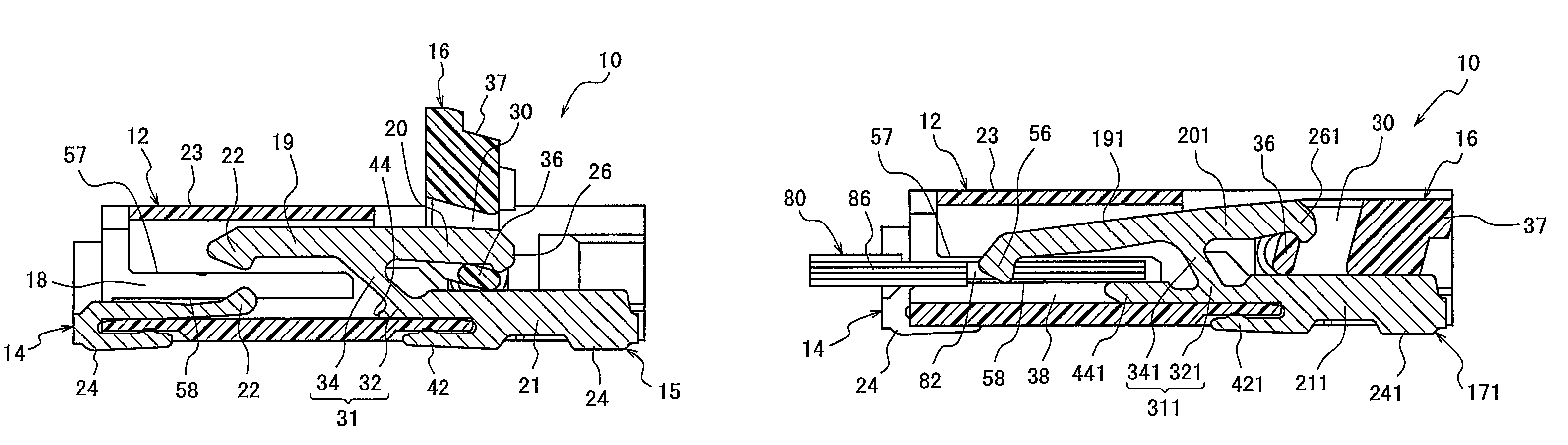
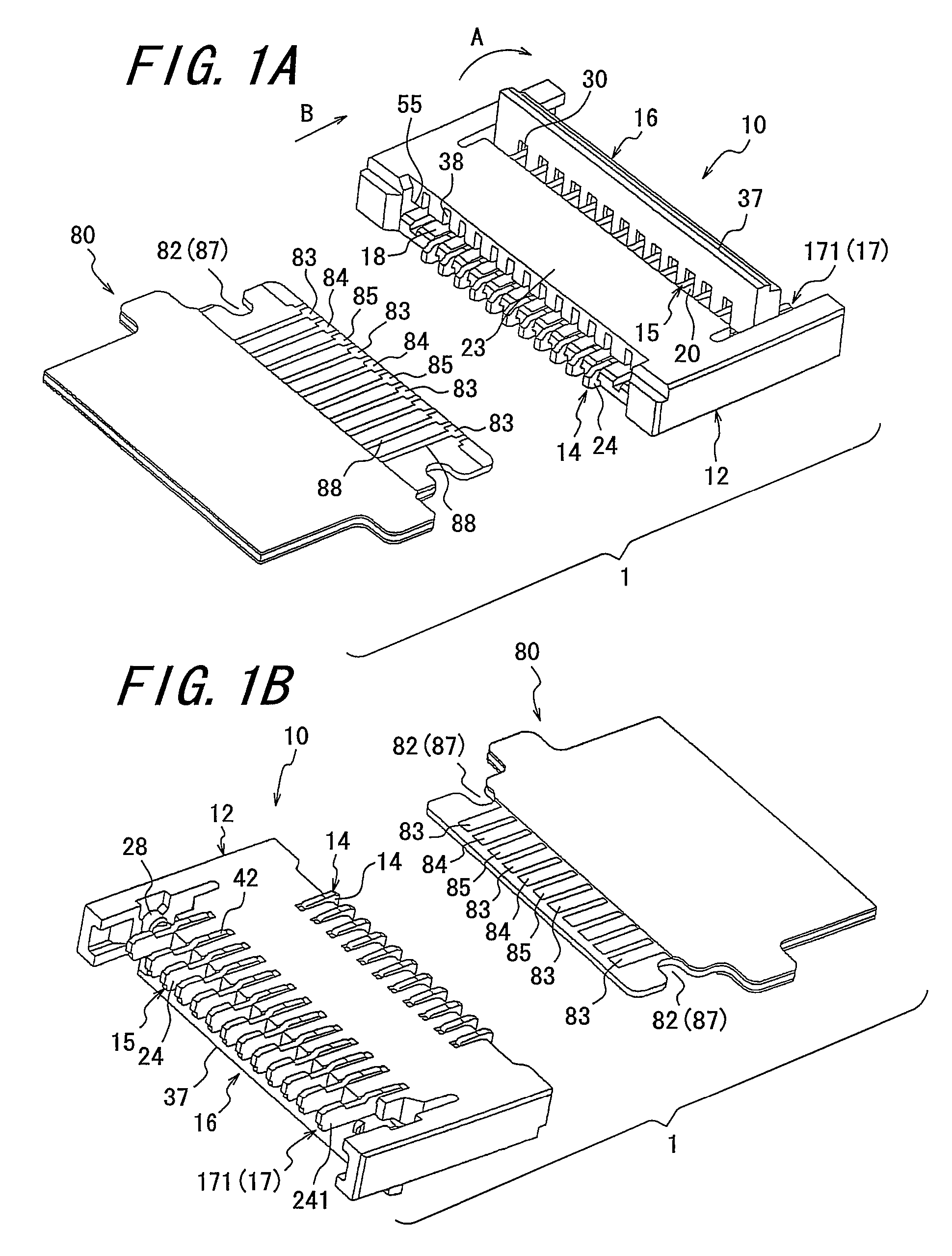
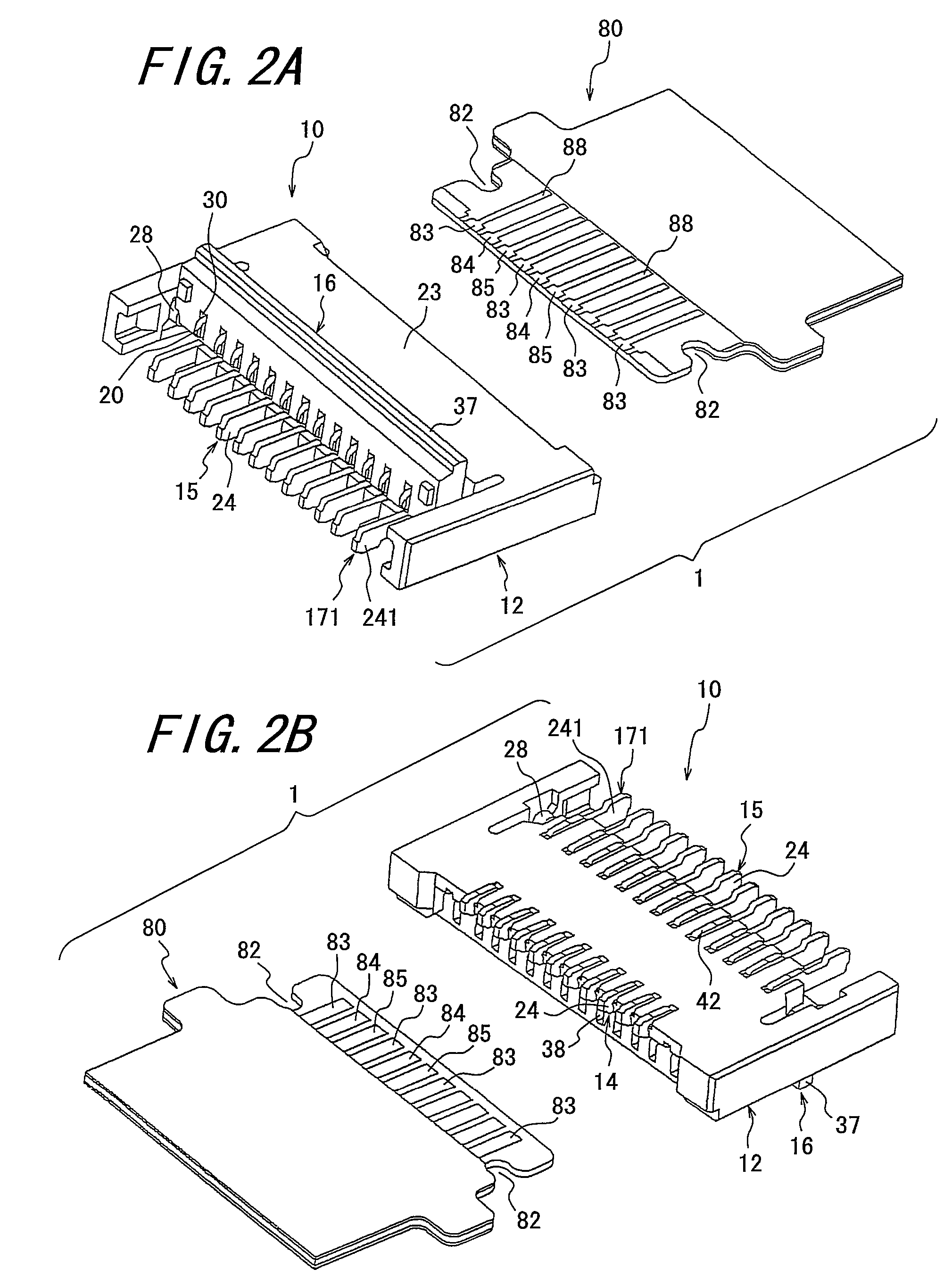
[0087]The important aspect of the invention lies in that a flexible printed circuit board 80 is provided with required numbers of ground patterns 83, signal patterns 84 and phase inversion signal patterns 85 whose phases are inverted, and with a ground layer 86 between said front and rear surfaces, the signal pattern 84 and the phase inversion signal pattern 85 being arranged between the ground patterns 83, and the flexible printed circuit board 80 is provided at predetermined positions with exposed portions 87 (recessed portions 871) which reach said ground layer 86, that the contacts of the connector 10 consist of first contacts 14 and second contacts 15 of two kinds, and one first contact 14 and one second contact 15 are arranged in one and the same inserting hole 38 such that the contact portions 22 of the first contact 14 and the second contact 15 are opposite to each other for using these contacts as an upper and lower contact structure. The connector 10 further includes a piv...


PUM


Abstract

A connector device to be used with a flexible printed circuit board including a connector. The flexible printed circuit board has on its front and rear surfaces ground patterns, signal patterns and phase inversion signal patterns arranged such that the signal pattern and the phase inversion signal pattern are arranged between the two ground patterns, and has a ground layer between the front and rear surfaces and exposed portions located at predetermined positions and reaching the ground layer. The connector has first and second contacts of two kinds. The first and second contacts are arranged in one and the same inserting hole of the housing such that their contact portions are opposite to each other. When a pivoting member has been pivotally moved, the first and second contacts come into contact with the corresponding ground, signal and phase inversion signal patterns on the flexible printed circuit board and the members at the predetermined positions enter the exposed portions so as to contact the ground layer, thereby achieving a miniaturization of the connector and high speed transmission of signals.

Description

BACKGROUND OF THE INVENTION[0001]This invention relates to a connector device for use in electric and electronic appliances such as mobile or cellular phones, notebook personal computers, digital cameras, and the like, and more particularly to a connector device with a structure achieving a miniaturization of the connector (high density of conductors) and at the same time high speed transmission of signals by causing respective contacts to come into contact with contact portions of a flexible printed circuit board and simultaneously causing members to be in contact with a ground layer arranged between a front and a rear surface of the flexible printed circuit board by pivotal movement of a pivoting member after the flexible printed circuit board has been inserted into the connector.[0002]A connector generally comprises at least a plurality of contacts, a housing for arranging and holding the contacts, and a pivoting member mounted on the housing for causing the contacts to be elasti...

Claims


Application Information

Patent Timeline
Patent Type & Authority Patents(United States)
IPC IPC(8): H01R13/15H01R12/59H01R12/82H01R24/40
CPCH01R12/79H01R12/88H01R12/57
Inventor SUZUKI, MASAYUKIKOYASU, OSAMU
Owner DDK LTD
Why Eureka
Try Eureka