
Sealed-by-resin type semiconductor device

a semiconductor device and resin-type technology, applied in semiconductor devices, semiconductor/solid-state device details, electrical equipment, etc., can solve the problems of large resin portion becoming a large restriction against product miniaturization, deterioration of the electric insulating resistance between the terminals, and the width of the sealing region for protecting the semiconductor element, so as to reduce the outside dimensions of the semiconductor device, the flexible region is larger, and the region width of the sealing region is reduced

Active Publication Date: 2010-08-03
SHENZHEN TOREY MICROELECTRONIC TECH CO LTD
View PDF32 Cites 3 Cited by
  • Summary
  • Abstract
  • Description
  • Claims
  • Application Information

AI Technical Summary

Benefits of technology

The present invention provides a semiconductor device and a method of manufacturing it that reduces the width of the sealing resin used to protect the semiconductor element, allowing for a smaller semiconductor device. This is achieved by applying the sealing resin along one longitudinal side of the semiconductor element, and forming peripheral resin portions on the other longitudinal sides that are not more than 1.0 mm in width from the semiconductor element. The sealing resin used has a low viscosity, making it easier to apply and flex. The reduced width of the sealing resin and the resulting smaller semiconductor device make it more convenient to use in various applications.

Problems solved by technology

If the resin sealing section was bent beyond its limit, such problems would be caused such as causing a crack in the sealing resin, pealing the sealing resin off from the flexible substrate.
Thus, a large resin portion becomes a large restriction against product miniaturization.
The migration leads to deterioration of the electric insulating resistance between the terminals.
Moreover, the conventional sealing resin has a high viscosity that gives the conventional sealing resin a poor flowability.
Such failing in filling, such as leaving the wiring patterns 102 or 103 uncovered leads to a qualitative problem.
Moreover, the viscosity of the sealing resin is 1000 mPa·S at 25° C., which is so high to give the sealing resin a poor flowability.
This results in a lower flowability and shorter pot life of the sealing resin, thereby deteriorating workability.

Method used


Image

  • Sealed-by-resin type semiconductor device
  • Sealed-by-resin type semiconductor device
  • Sealed-by-resin type semiconductor device

Examples


example

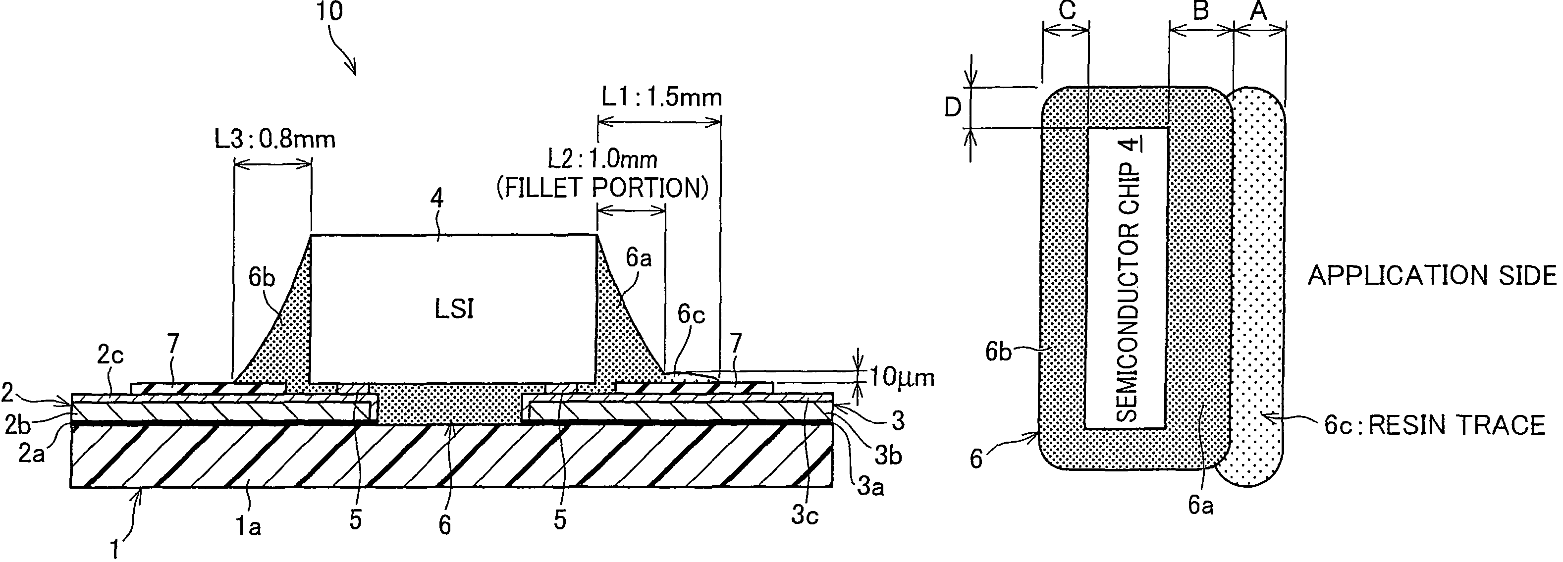
[0082]For the production of the semiconductor device 10, a sealing resin was applied in a constant quantity via the nozzle 41 along one side of the semiconductor chip 4 as illustrated in FIG. 4(a). The sealing resin contained the coloring agent by 0.15 wt % and had a viscosity of 400 mPa·s at 25° C., as shown in Table 3. The application of the resin was preceded by preheating the semiconductor chip 4 to 90° C. by using a heater, in order to increase the flowability of the sealing resin that would be the under-fill 6 in the gap between the semiconductor chip 4 and the flexible wiring substrate.

[0083]Next, in order to stabilize shapes of the fillets 6a and 6b and the resin trace 6c and to harden the resin, the semiconductor device 10 is treated for a predetermined time enough for the curing the resin, in a curing oven whose temperature is increased to a predetermined temperature with a hot-air circulation or far infra-red heater. Thereby, the curing of the sealing resin is completed.

[...


PUM


Abstract

A semiconductor device such as a COF or the like is provided on a semiconductor chip on a film-like shaped flexile wiring substrate on which a wiring pattern is formed. Between the semiconductor chip and the flexile wiring substrate, a sealing resin is filled for protecting the semiconductor chip. In the semiconductor device, a resin trace is 0.1 to 1.0 mm in width and 10 μm in thickness, the resin trace being formed when applying the sealing resin along a longitudinal side of the semiconductor chip.

Description

[0001]This Nonprovisional application claims priority under 35 U.S.C. §119(a) on Patent Application No. 027056 / 2005 filed in Japan on Feb. 2, 2005, the entire contents of which are hereby incorporated by reference.FIELD OF THE INVENTION[0002]The present invention relates to a semiconductor device called COF (Chip On Film), the semiconductor device including a semiconductor element on a flexible wiring substrate.[0003]The present invention is applicable to a tape-carrier-package type semiconductor device called COF (Chip On Film), and a manufacturing method thereof. The Semiconductor device is arranged such that a wiring pattern on a flexible film is connected with an electrode of at least one semiconductor element, the electrode being for connecting the semiconductor element with an external circuit. An example of usage of the COF is a liquid crystal driver in which the semiconductor element servers as a liquid crystal driver IC and mounted on a flexible wiring substrate.[0004]Moreo...

Claims


Application Information

Patent Timeline
Patent Type & Authority Patents(United States)
IPC IPC(8): H01L23/48
CPCH01L21/563H01L23/4985H01L2924/07811H01L2924/12041H01L2224/73204H01L2224/32225H01L2224/16225H01L2224/73203H01L2924/01078H01L2924/01079H01L2924/12044H01L2924/3011H01L2924/00H01L2924/00011H01L2924/00014H01L2224/0401H01L23/12
Inventor FUKUTA, KAZUHIKOTOYOSAWA, KENJI
Owner SHENZHEN TOREY MICROELECTRONIC TECH CO LTD
Learn More