Modeling power management for an integrated circuit

a power management and integrated circuit technology, applied in the field of integrated circuit power management design, can solve the problems of not being able to capture the intended behavior in the rtl of the design, not being able to implement certain power management techniques at the physical level after circuit synthesis, and unable to meet the requirements of design verification

Inactive Publication Date: 2010-08-03
CADENCE DESIGN SYST INC
View PDF7 Cites 30 Cited by
  • Summary
  • Abstract
  • Description
  • Claims
  • Application Information

AI Technical Summary

Problems solved by technology

This phenomenon has resulted in substantial design and verification challenges for low-power applications, and as a result designers are increasingly turning towards advanced verification methodologies, such as coverage driven verification, and verification planning.
Such power management issues become even more critical in view of the continuous shrinking of device dimensions with the next generation of semiconductor processing technology.
Certain power management techniques can only be implemented at the physical level after circuit synthesis.
These power management design techniques may significantly change the design intent, yet none of the intended behavior can be captured in the RTL of the design.
This deficiency creates a gap in the RTL to Graphic Data System II (GDSII) implementation and verification flow where the original RTL can no longer be relied upon as a correct representation of the design, and thus cannot be used to verify the final netlist implementation containing power management implementations.

Method used


Image

  • Modeling power management for an integrated circuit
  • Modeling power management for an integrated circuit
  • Modeling power management for an integrated circuit

Examples


Embodiment Construction

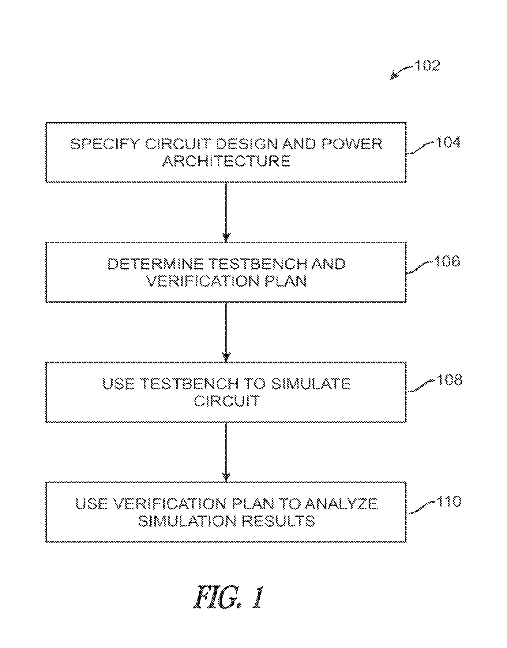
[0036]An embodiment of the present invention is shown in FIG. 1. A method 102 for modeling power management in an integrated circuit (IC) includes: specifying a circuit design and a power architecture for the IC 104, where the power architecture includes multiple power domains for specifying power levels in different portions of the IC; determining a testbench for simulating the IC and a verification plan for evaluating simulation results 106; using the testbench to simulate variations in power levels of the power domains of the IC 108; and using the verification plan to evaluate the simulation results for the power domains of the IC 110. Additional exemplary details for each step are provided below.

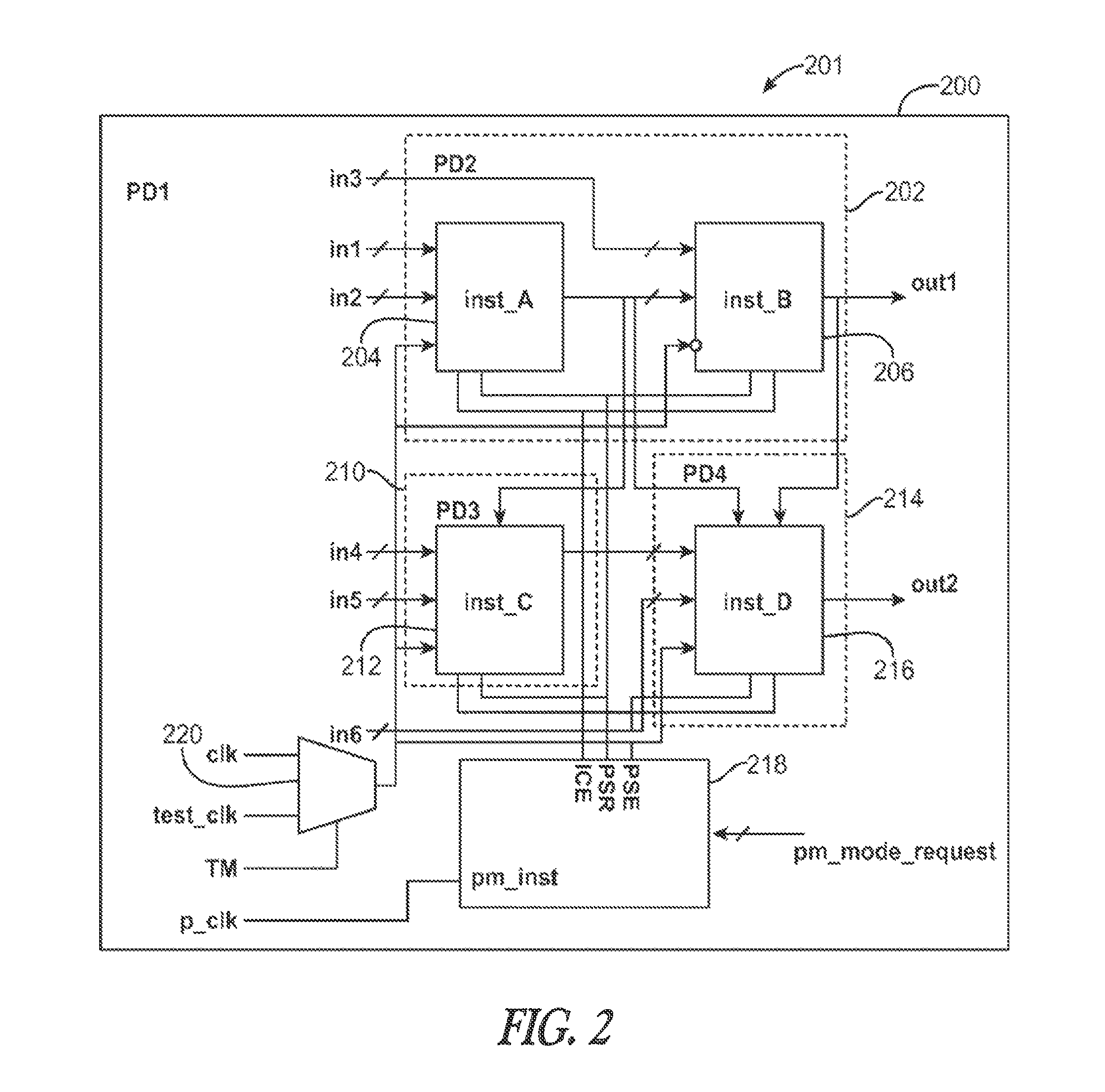
[0037]FIGS. 2-4 show details related to specifying a circuit design and power architecture for the IC 104. FIG. 2 shows an exemplary IC 201 with power domains PD1200, PD2202, PD3210, and PD4214, where PD1 is a system-level power domain that includes PD2, PD3, and PD4 and additional syste...


PUM


Abstract

A method for modeling power management in an integrated circuit (IC) includes: specifying a circuit design and a power architecture for the IC, the power architecture including a plurality of power domains for specifying power levels in different portions of the IC; determining a testbench for simulating the IC and a verification plan for evaluating simulation results; using the testbench to simulate variations in power levels of the power domains of the IC; and using the verification plan to evaluate the simulation results for the power domains of the IC.

Description

CROSS-REFERENCE TO RELATED APPLICATIONS[0001]This application claims the benefit of U.S. Provisional Application No. 60 / 855,443, filed Oct. 30, 2006, entitled METHOD AND APPARATUS FOR DEVELOPING TEST BENCH FOR LOW-POWER DESIGN, and incorporated herein by reference in its entirety.[0002]This application is related to commonly owned U.S. Provisional Application No. 60 / 792,060, filed Apr. 14, 2006, and entitled METHOD AND MECHANISM FOR IMPLEMENTING ELECTRONIC DESIGNS HAVING POWER INFORMATION SPECIFICATIONS, U.S. Ser. No. 11 / 489,384, filed Jul. 18, 2006, and entitled METHOD AND SYSTEM FOR SIMULATING STATE RETENTION OF AN RTL DESIGN, and U.S. Ser. No. 11 / 489,385, filed Jul. 18, 2006, and entitled SIMULATION OF POWER DOMAIN ISOLATION, each of which is expressly incorporated herein by reference in its entirety.BACKGROUND OF THE INVENTION[0003]1. Field of Invention[0004]The present invention relates to integrated circuits and more particularly to power-management design of integrated circui...

Claims


Application Information

Patent Timeline
Patent Type & Authority Patents(United States)
IPC IPC(8): G06F17/50
CPCG06F17/5036G06F30/367
Inventor SHMAYOVITSH, ARIKDECKER, JOHNLEIBOVICH, DAN
Owner CADENCE DESIGN SYST INC
Why Eureka
Try Eureka