
Memory device having wide area phase change element and small electrode contact area

a phase change element and memory device technology, applied in semiconductor devices, digital storage, instruments, etc., can solve the problems of manufacturing such devices with very small dimensions, and achieve the effect of high repeatability, readily and repeatably controlled

Active Publication Date: 2010-08-10
MACRONIX INT CO LTD
View PDF241 Cites 98 Cited by
  • Summary
  • Abstract
  • Description
  • Claims
  • Application Information

AI Technical Summary

Benefits of technology

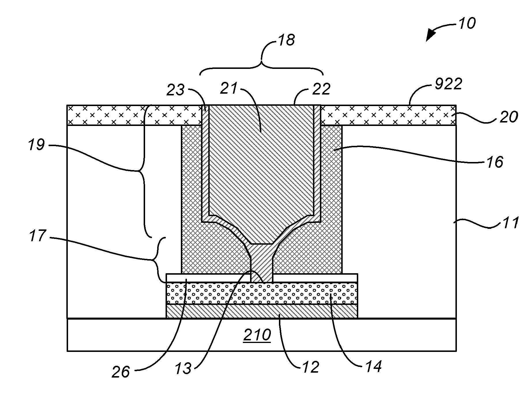
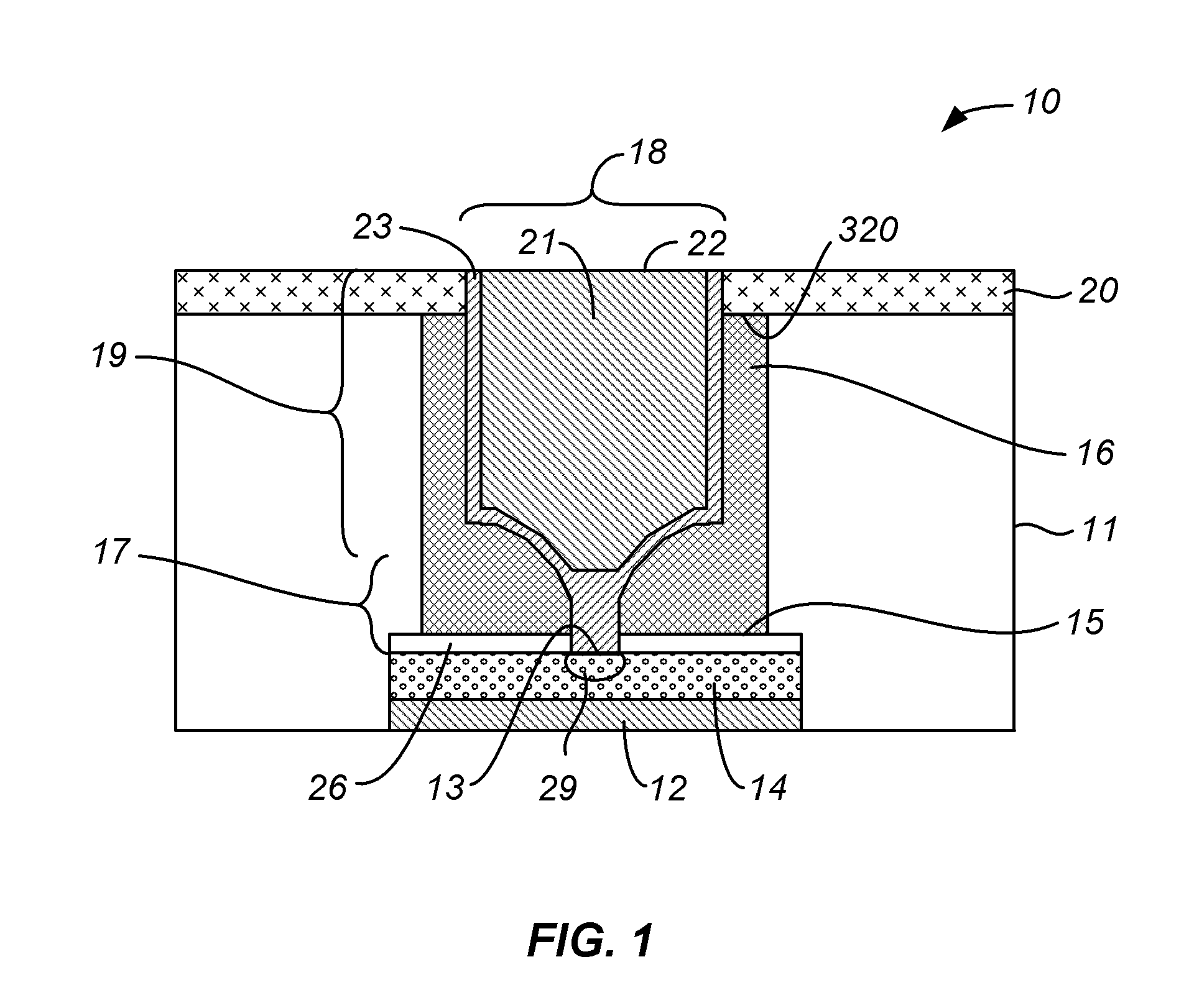
[0013]According to the invention, a masking step establishes the openings in the silicon nitride layer over the memory cell vias. The remainder of the process is self-aligning, and highly repeatable. The area of contact between the top electrode and the memory material is determined by width of the stem portion of the top electrode, which in turn is determined by anisotropic etch conditions and by the size and shape of the void in the thermal insulator, which can be readily and repeatably controlled.

Problems solved by technology

Problems have arisen in manufacturing such devices with very small dimensions, and with variations in process that meet tight specifications needed for large-scale memory devices.

Method used


Image

  • Memory device having wide area phase change element and small electrode contact area
  • Memory device having wide area phase change element and small electrode contact area
  • Memory device having wide area phase change element and small electrode contact area

Examples


Embodiment Construction

[0019]The invention will now be described in further detail by reference to the drawings, which illustrate alternative embodiments of the invention. The drawings are diagrammatic, showing features of the invention and their relation to other features and structures, and are not made to scale. For improved clarity of presentation, in the FIGs. illustrating embodiments of the invention, features corresponding to features shown in other drawings are not all particularly renumbered, although they are all readily identifiable in all the FIGs.

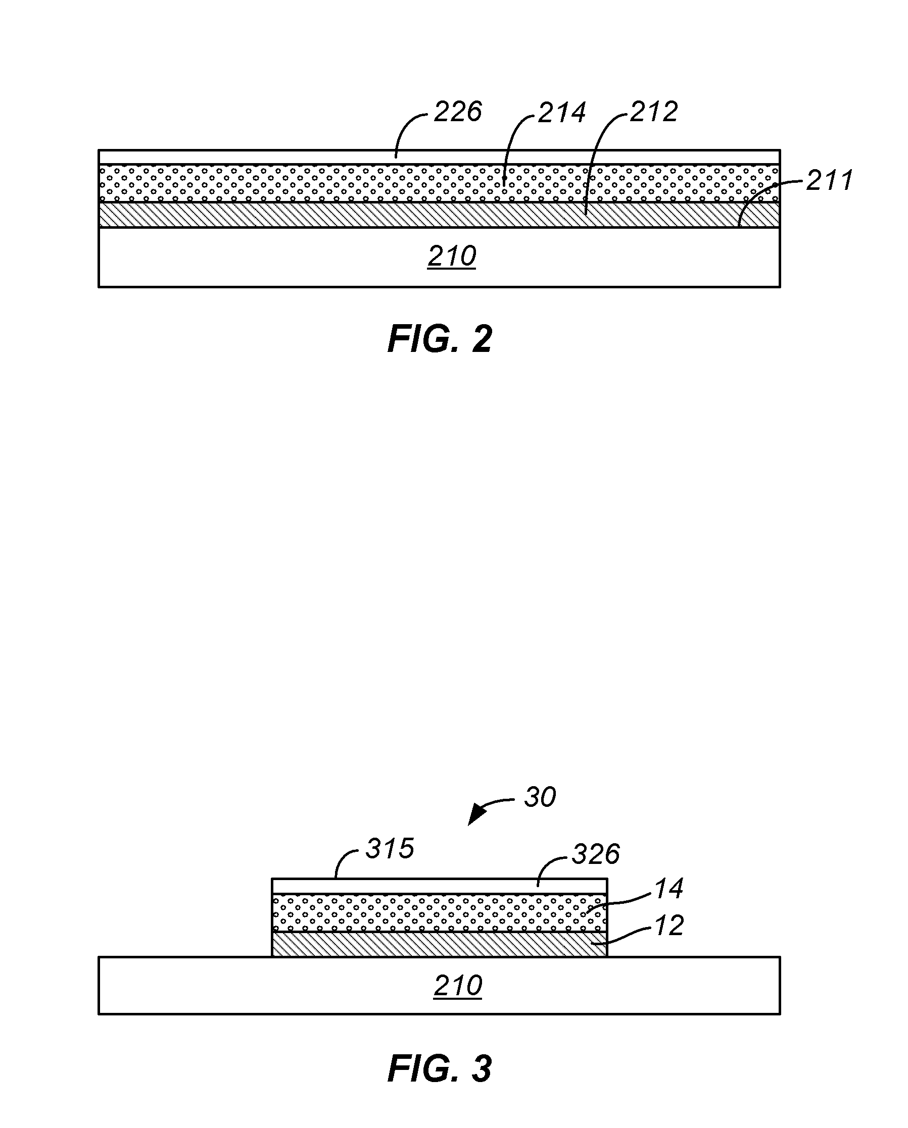
[0020]Turning now to FIG. 1, there is shown generally at 10 a memory cell structure according to an embodiment of the invention. Memory cell structure 10 includes a bottom electrode 12 overlain by a memory element 14, a top electrode 18 including a body portion 19 and a stem portion 17. The stem portion 17 of the top electrode 18 is in contact with a small area 13 of the surface 15 of the memory material layer 14. The top electrode may optionally inc...


PUM


Abstract

A memory cell device of the type that includes a memory material switchable between electrical property states by application of energy, situated between first and second (“bottom” and “top”) electrodes has a top electrode including a larger body portion and a stem portion. The memory material is disposed as a layer over a bottom electrode layer, and a base of the stem portion of the top electrode is in electrical contact with a small area of the surface of the memory material. Methods for making the memory cell are described.

Description

PARTIES TO A JOINT RESEARCH AGREEMENT[0001]International Business Machines Corporation, a New York corporation, Macronix International Corporation, Ltd., a Taiwan corporation, and Infineon Technologies A.G., a German corporation, are parties to a Joint Research AgreementBACKGROUND[0002]1. Field of the Invention[0003]This invention relates to high density memory devices based on phase change based memory materials, including chalcogenide based materials and other materials, and to methods for manufacturing such devices.[0004]2. Description of Related Art[0005]Phase change based memory materials are widely used in read-write optical disks. These materials have at least two solid phases, including for example a generally amorphous solid phase and a generally crystalline solid phase. Laser pulses are used in read-write optical disks to switch between phases and to read the optical properties of the material after the phase change.[0006]Phase change based memory materials, like chalcogen...

Claims


Application Information

Patent Timeline
Patent Type & Authority Patents(United States)
IPC IPC(8): H01L29/04
CPCG11C11/5678H01L27/2436H01L45/06H01L45/1233H01L45/126H01L45/143H01L45/144H01L45/148H01L45/1675G11C13/0004G11C2213/79H10B63/30H10N70/231H10N70/8413H10N70/8825H10N70/826H10N70/884H10N70/8828H10N70/063
Inventor LUNG, HSIANG-LAN
Owner MACRONIX INT CO LTD
Learn More