Stacked semiconductor structure and fabrication method thereof

a technology of semiconductor structure and fabrication method, which is applied in the direction of semiconductor device, semiconductor/solid-state device details, electrical apparatus, etc., can solve the problems of reducing product yield and product reliability, affecting reducing the number of electrical i/o, so as to improve the electrical function of stacked semiconductor structure, shorten the length of bonding wire, and eliminate the effect of electrical i/o

Active Publication Date: 2010-08-10
SILICONWARE PRECISION IND CO LTD
View PDF4 Cites 37 Cited by
  • Summary
  • Abstract
  • Description
  • Claims
  • Application Information

AI Technical Summary

Benefits of technology

[0013]Accordingly, it is a primary objective of the present invention to provide a stacked semiconductor structure and a fabrication method thereof without limiting the size and type of stacked packages and the number of electrical I / O.
[0014]It is another objective of the present invention to provide a stacked semiconductor device and a fabrication method thereof, which avoids the use of a reflow process for electrical connection between stacked substrates and thus prevents the contamination of a semiconductor chip.
[0015]It is yet another objective of the present invention to provide a stacked semiconductor structure and a fabrication method thereof, which prevents a fabrication cost increase problem due to a special mold used.
[0016]It is a further objective of the present invention to provide a stacked semiconductor structure and a fabrication method thereof, which prevents a stacked substrate from flash-related contamination during a molding process.
[0019]Furthermore, in other embodiments of the stacked semiconductor structure and fabrication method thereof according to the present invention, the method can also include attaching and electrically connecting at least one semiconductor chip, a passive component or a package to the second surface of the second substrate before mounting the second substrate, via the second surface of the second substrate, on the supporting members disposed on the first substrate, so as to enhance electrical functions of the stacked semiconductor structure. Moreover, each of the supporting members can be a scrap chip, a metal block, an insulating block, a substrate piece or the like. Therein, if the substrate pieces are used as the supporting members, by electrically connecting the supporting members to the second substrate and the first substrate respectively, the supporting members can function as an electrical bridge between the first and second substrates, thereby shortening the length of the bonding wires required for direct electrical connection between the second substrate and the first substrate.
[0020]Thus, according to the stacked semiconductor structure and fabrication method thereof of the present invention, since the solder pads on the first surface of the second substrate are completely exposed from the encapsulant, conventional limitation on the size and type of stacked packages and the number of electrical I / O is eliminated. Moreover, by electrically connecting the second substrate and the first substrate through a wire bonding process instead of a reflow process, the known contamination problem with a semiconductor chip is overcome. Further, by disposing the tape on the second substrate before performing a molding process, the present invention avoids the use of the special mold of the prior art, thereby decreasing the fabrication cost and preventing the flash-induced contamination problem of the second substrate.

Problems solved by technology

However, to form the above stacked semiconductor package structure, a reflow process is performed to electrically connect the second BGA substrate 22 to the first BGA substrate 21 through solder balls 24 after the semiconductor chip 20 is electrically connected to the first BGA substrate 21 through bonding wires 25, which not only adversely affects quality of the bonding wires 25, but also brings about contamination of the semiconductor chip 20 and the first BGA substrate 21, thereby reducing product yield and product reliability.
However, the process cost increases because of the introduction of the metallic stiffener 37 into the above-described method.
Furthermore, the process cost increases also because the process involves using a special mold to prevent the bonding wires 352 on the substrate 32 from touching the mold.
In addition, during the molding process disclosed in U.S. Pat. Nos. 6,828,664 and 6,861,288, an encapsulant is likely to flash over and contaminate the second BGA substrate or the stacked substrate, thereby bringing trouble to subsequent processes such as a deflash process, a package stacking process and an electrical connection process.

Method used


Image

  • Stacked semiconductor structure and fabrication method thereof
  • Stacked semiconductor structure and fabrication method thereof
  • Stacked semiconductor structure and fabrication method thereof

Examples


first embodiment

[0034]With reference to FIGS. 4A through 4G, shown are cross-sectional views of a method of fabricating a stacked semiconductor structure.

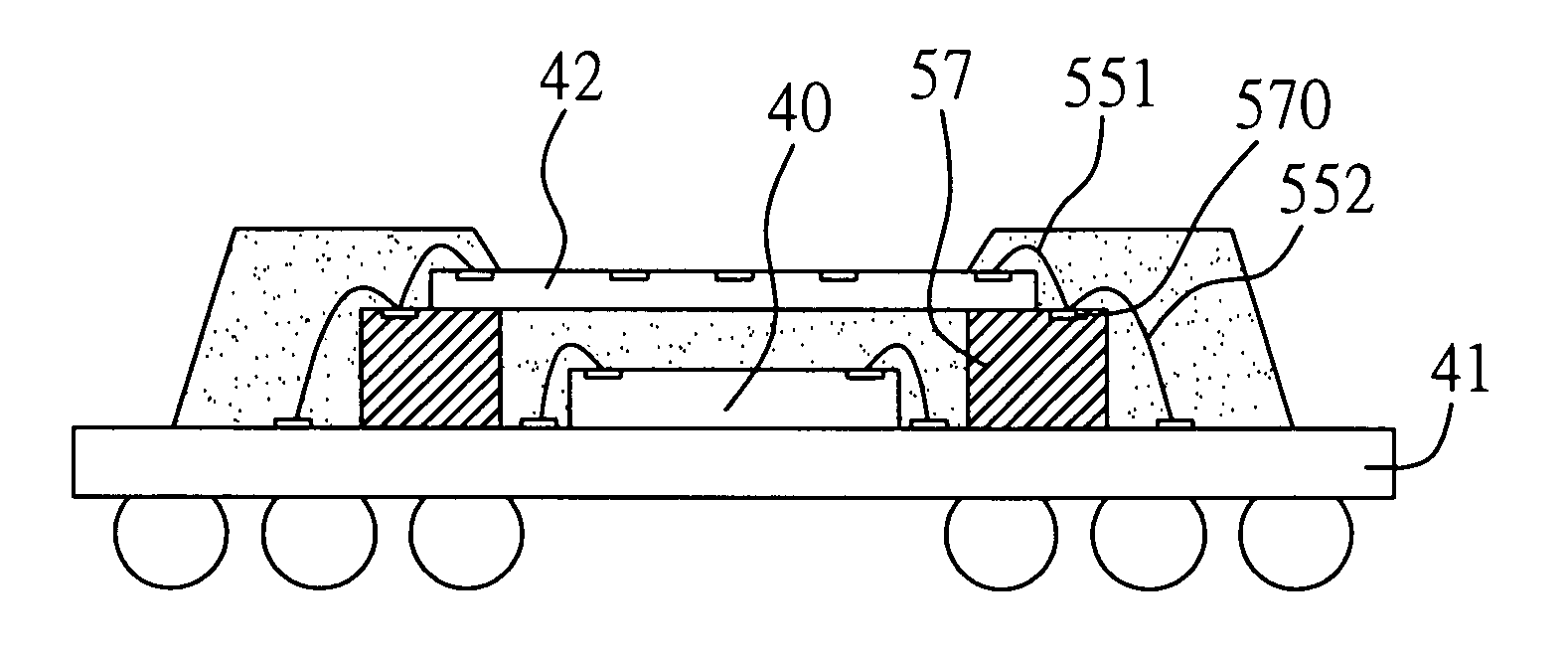
[0035]As shown in FIG. 4A, a first substrate 41 such as a BGA (Ball Grid Array) substrate is provided. At least one semiconductor chip 40 is mounted on and electrically connected with the first substrate 41, and a plurality of supporting members 47 are glued to the first substrate 41 such that the supporting members 47 correspond in position to a periphery of the semiconductor chip 40, using an adhesive (not shown), for example. The semiconductor chip 40 is electrically connected to the first substrate 41 through a plurality of bonding wires 451. The supporting members 47 can be such as a scrap chip, a metal block, and an insulating block. The supporting members 47 are higher than a loop of the bonding wires 451.

[0036]FIGS. 5A and 5B show a plan view of the first substrate 41 with the semiconductor chip 40 and the supporting members 47 mounted the...

second embodiment

[0046]FIG. 7 is a cross-sectional view of a stacked semiconductor structure according to the second embodiment of the present invention. The stacked semiconductor structure of the present embodiment is similar to that of the first embodiment. The main difference between the stacked semiconductor structure of the present embodiment and that of the first embodiment is that the semiconductor chip 40 is flip-chip mounted and electrically connected to the first substrate 41.

third embodiment

[0047]FIG. 8 is a cross-sectional view of a stacked semiconductor structure according to the third embodiment of the present invention. The stacked semiconductor structure of the present embodiment is similar to that of the first embodiment. The main difference between the stacked semiconductor structure of the present embodiment and that of the first embodiment is that a semiconductor chip 400 is mounted to the second surface 422 of the second substrate 42 and is flip-chip electrically connected to the second substrate 42 before the second substrate 42 is mounted to the supporting members 47 for further electrical connection. Thereby, the electrical function of the stacked semiconductor structure can be enhanced.


PUM


Abstract

A stacked semiconductor structure and fabrication method thereof are provided. The method includes mounting and connecting electrically a semiconductor chip to a first substrate, mounting on the first substrate a plurality of supporting members corresponding in position to a periphery of the semiconductor chip, mounting a second substrate having a first surface partially covered with a tape and a second surface opposite to the first surface on the supporting members via the second surface, connecting electrically the first and second substrates by bonding wires, forming on the first substrate an encapsulant for encapsulating the semiconductor chip, the supporting members, the second substrate, the bonding wires, and the tape with an exposed top surface, and removing the tape to expose the first surface of the second substrate and allow an electronic component to be mounted thereon. The present invention prevents reflow-induced contamination, spares a special mold, and eliminates flash.

Description

BACKGROUND OF THE INVENTION[0001]1. Field of the Invention[0002]The present invention relates generally to a semiconductor device and fabrication method thereof, and more particularly, to a stacked semiconductor structure and fabrication method thereof.[0003]2. Description of Related Art[0004]Given the trend toward multifunction, higher electrical performance and high-speed operation, more and more semiconductor devices integrated with a plurality of chips or packages are released.[0005]With reference to FIG. 1, U.S. Pat. No. 5,222,014 proposes a stacked semiconductor package structure, which includes a first ball grid array (BGA) substrate 11 having pads 110 provided on an upper surface thereof, a semiconductor chip 10 mounted on the first BGA substrate 11, an encapsulant 13 encapsulating the semiconductor chip 10, and a second packaged BGA substrate 12 mounted and electrically connected to the pads 110 of the first BGA substrate 11 through solder balls 14.[0006]However, in the abo...

Claims


Application Information

Patent Timeline
Patent Type & Authority Patents(United States)
IPC IPC(8): H01L23/02
CPCH01L21/561H01L21/565H01L23/16H01L23/3128H01L24/97H01L25/0657H01L2224/48091H01L2224/48235H01L2224/73265H01L2224/97H01L2225/0651H01L2225/06513H01L2225/06517H01L2225/06527H01L2225/06572H01L2225/06586H01L2924/15174H01L2924/15311H01L2924/15331H01L2924/00014H01L2224/85H01L24/48H01L2924/01033H01L2224/16225H01L2224/32225H01L2224/48227H01L2924/1815H01L2924/19107H01L2924/00H01L2924/00012H01L24/73H01L2924/181H01L24/49H01L2224/49175H01L2224/45099H01L2224/45015H01L2924/207
Inventor HUANG, CHIEN-PINGHUANG, CHIH-MINGPU, HAN-PINGWANG, YU-POHSIAO, CHENG-HSU
Owner SILICONWARE PRECISION IND CO LTD
Why Eureka
Try Eureka