Data processing apparatus including reconfigurable logic circuit

a logic circuit and data processing technology, applied in the field of data processing apparatus including reconfigurable logic circuits, can solve the problems of ineffective application of the conventional art described above, meaningless processing cannot be carried out, etc., and achieve the effect of reducing the number of types of logic elements, reducing the size of cb mapping information, and reducing the number of logic elements

Active Publication Date: 2010-08-17
TOKYO KEIKI
View PDF20 Cites 23 Cited by
  • Summary
  • Abstract
  • Description
  • Claims
  • Application Information

AI Technical Summary

Benefits of technology

[0004]One of aspects of the present invention is providing a technology for implementing a circuit for carrying out an application in hardware that can be reconfigured on a cycle basis. For such hardware, the circuit configuration can be changed in every cycle. Accordingly, it becomes possible to not only carry out dynamic reconfiguring at the functional module level in units of 500 to 1000 cycles using the conventional art described above, but also to carry out reconfiguring in more precise time units or cycles, thereby increasing the range for which dynamic reconfiguring can be applied. By quantitatively changing the reconfiguration time from several tens of cycles to just one cycle, the usage of such reconfiguration qualitatively changes from the functional module level to the behavior (action and / or response) state level. One of other aspects of this invention is providing control information and a method suited to control of a data processing system (apparatus, device) equipped with a reconfigurable logic circuit.
[0014]Accordingly, the configuration of the CB circuits mapped on a reconfigurable logic circuit is a simple configuration that expresses only the parts of data paths that are required in each cycle and fundamentally does not include selectors and the like for switching inputs, and can be implemented with fewer logic elements. Also, selector control signals for switching the input of logic elements to select the logic are not required, and instead logic is selected according to configuration selection information that selects the CB mapping information according to the execution state of the application. Therefore, according to the present invention, it is possible to change a reconfigurable circuit region from being used at a functional module level to being used at a behavior state level.
[0015]The method should preferably include a step of generating composite cycle-based mapping information that includes extracting, out of the plurality of pieces of cycle-based mapping information, some pieces cycle-based mapping information that are capable of being merged without obstructing the functions in each cycle and merging two or more pieces cycle-based mapping information extracted. This step is carried out not to combine circuits across cycles in accordance with signals transmitted between cycles but to reduce the number of types of pieces of CB mapping information and to reduce the size of the CB mapping information required to execute the application. Accordingly, instead of selecting and merging cycle adjacent pieces of CB mapping information as the timing for mapping, merging includes (i) the merging of information that have non-consecutive timing but share common features in the configuration of the CB circuits to generate piece of composite CB mapping information equipped with circuit that is not required for the functions in a given cycle but does not obstruct such functions, and (ii) the merging of smaller pieces of CB mapping information to generate an independent CB circuit expressed by one piece of composite CB mapping information.

Problems solved by technology

Although an FPGA might be capable of dynamically reconfigurable, at least several tens of cycles will be required by programming, during which time meaningful processing cannot be carried out.
When reconfiguring on this type of functional module level is not possible or useful for an application, applying the conventional art described above is not effective.

Method used


Image

  • Data processing apparatus including reconfigurable logic circuit
  • Data processing apparatus including reconfigurable logic circuit
  • Data processing apparatus including reconfigurable logic circuit

Examples


Embodiment Construction

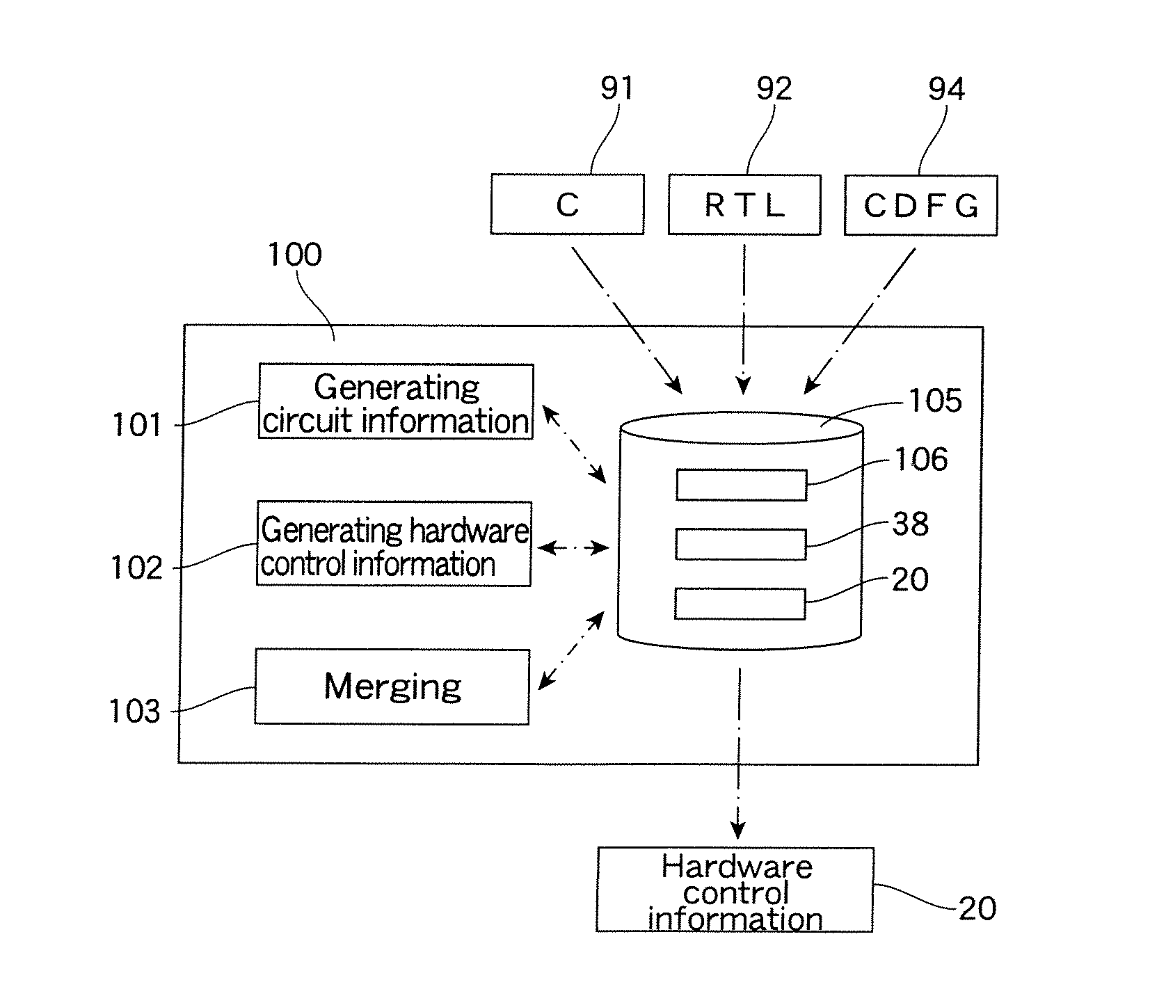
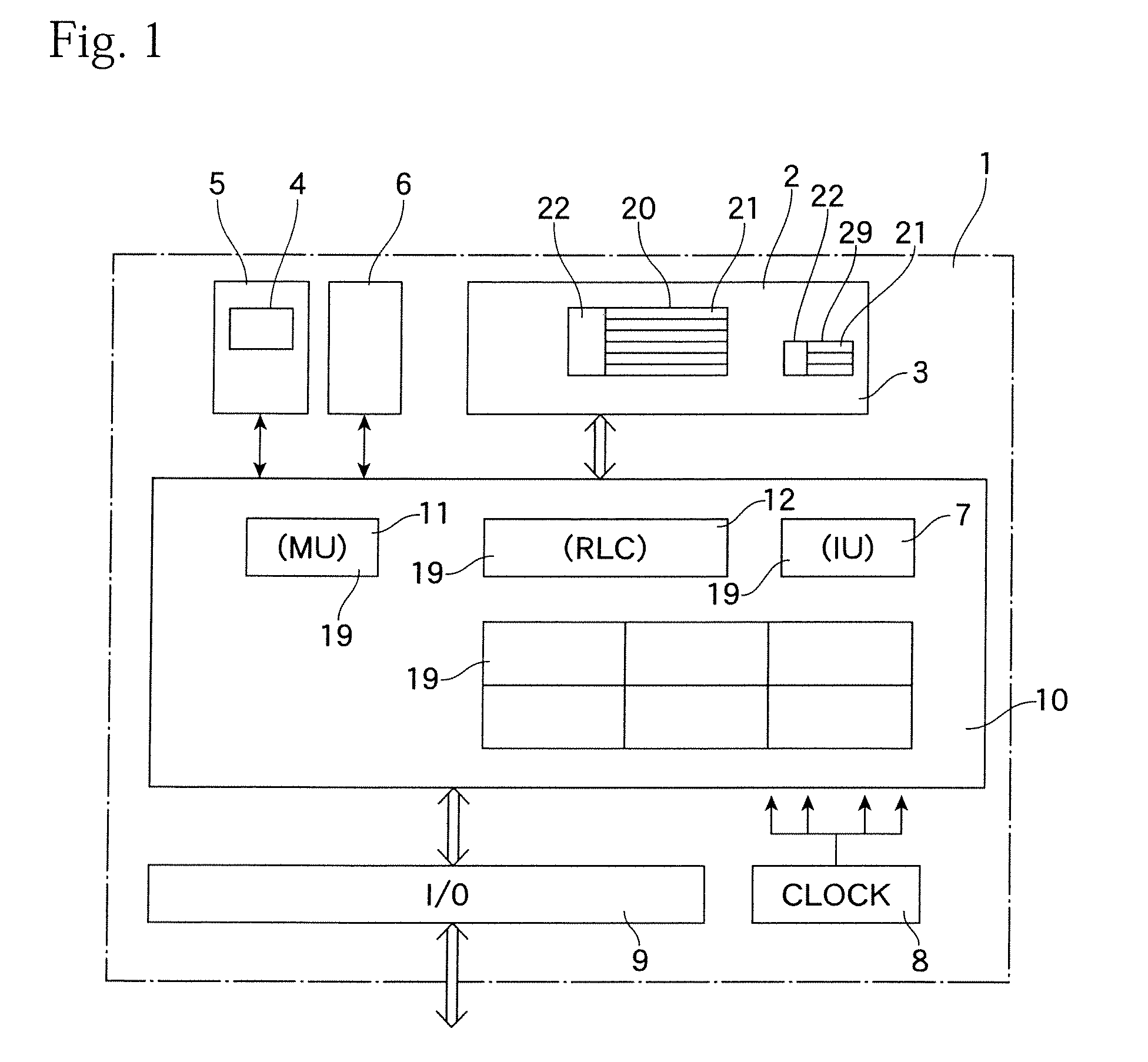
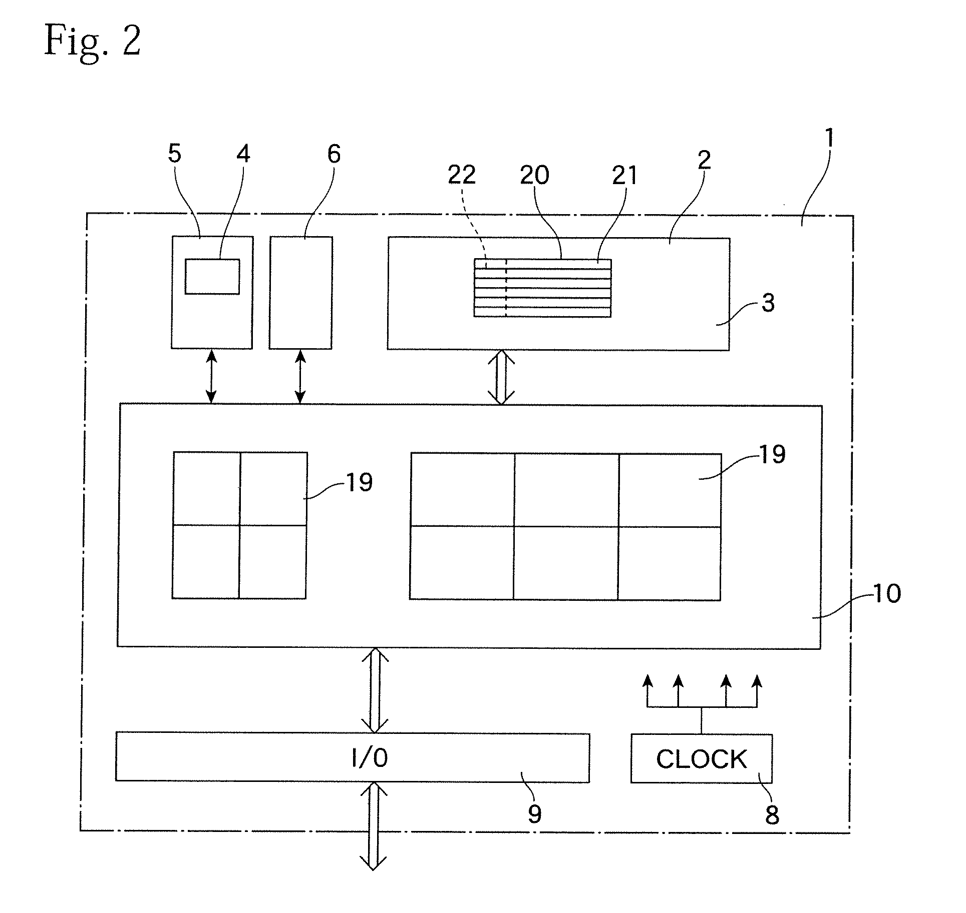
[0047]A data processing apparatus (system) 1 shown in FIG. 1 is an electronic device, such as an LSI, IC, chip, or chipset and is equipped with a logic circuit region (or “RC region” or “reconfigurable region”) 10 in which circuits can be dynamically reconfigured and a memory 3 for a library 2 in which hardware control information 20 for executing a number of applications is stored (recorded). The same type system as the data processing apparatus 1 may be constructed as an optical device or an electro-optical device. This data processing apparatus 1 further includes a mapping unit (MU) 11. The MU 11 is a control unit for reconfiguring cycle-based circuits (CB circuits) 19 by obtaining (“fetching” or “downloading”) desired piece or pieces of cycle-based mapping information (CB mapping information) 21 out of the hardware control information 20 from the library 2 and mapping the CB mapping information 21 onto the RC region 10 or a suitable region that is part of the RC region 10. The d...


PUM


Abstract

There is provided a data processing apparatus (1) including a logic circuit (10) that is reconfigurable in each cycle and a library (2) that stores hardware control information (20). The hardware control information (20) includes a plurality of pieces of cycle-based mapping information (21) for individually mapping a plurality of cycle-based circuits, which each realize a function in each cycle for executing an application, onto the logic circuit (10) and configuration selection information (22) for selecting at least one of the plurality of pieces of cycle-based mapping information according to an execution state of the application. The data processing apparatus (1) includes a control unit (11) that reconfigures at least part of the logic region (10) using at least one of the plurality of pieces of cycle-based mapping information (21) according to a request in each cycle based on the configuration selection information (22).

Description

TECHNICAL FIELD[0001]The present invention relates to a data processing apparatus including a reconfigurable logic circuit.BACKGROUND ART[0002]An FPGA (Field Programmable Gate Array) is known as a programmable device in which circuits can be reconfigured. As one technology that implements different parts of a logic circuit in an FPGA, Japanese Laid-Open Patent Publication No. 2000-40745 discloses a technology for dividing an initial net list that defines the logic circuit into many pages and implements a circuit for one of such pages in the FPGA. By doing so, this technology aims to make it possible to implement a much larger circuit than the physical capacity of the FPGA. Japanese Laid-Open Patent Publication No. 2003-518666 discloses a technology that divides a design net list into sets of static macros and sets of reconfigurable macro contexts, compiles the respective reconfigurable contexts, and carries out placing and routing for the initial device contexts.DISCLOSURE OF THE IN...

Claims


Application Information

Patent Timeline
Patent Type & Authority Patents(United States)
IPC IPC(8): G06F17/50
CPCG06F17/5054G06F15/7867G06F30/34G06F11/261G06F30/33G06F30/331G06F30/347G06F30/3308
Inventor HONDA, HIROKI
Owner TOKYO KEIKI
Why Eureka
Try Eureka