Method for manufacturing cathode assembly of field emission display

a technology of field emission display and cathode assembly, which is applied in the manufacture of electrode systems, electrode discharge tubes/lamps, nanoinformatics, etc., can solve the problems of reducing power utilization efficiency, requiring more time, and requiring more time, so as to reduce the probability of carbon nanotubes being shorted between the gate electrode layer and the carbon nanotubes, and preventing carbon nanotubes from contacting

Active Publication Date: 2010-08-31
TSINGHUA UNIV +1
View PDF11 Cites 43 Cited by
  • Summary
  • Abstract
  • Description
  • Claims
  • Application Information

AI Technical Summary

Benefits of technology

[0012]The method deposits the catalyst layer through the at least one opening defined by the pressed photoresist layer. Since the at least one gate electrode opening is larger than the at least one opening in the pressed photoresist layer, the catalyst layer is smaller than the at least one gate electrode opening, and a region of the grown carbon nanotubes from the catalyst layer is smaller than the at least one gate electrode opening. Therefore, the cathode assembly efficiently prevents carbon nanotubes contacting with the gate electrode layer. The probability of shorting between the gate electrode layer and the carbon nanotubes is thus decreased. Furthermore, the probability of electrons emitted from the carbon nanotubes being transmitted to the gate electrode layer is decreased. The method is simple and can be performed without using additional material, and as a result the cost is low.

Problems solved by technology

The mechanical method is simple, but it is more difficult to operate and requires more time.
Especially, if the diameter of the carbon nanotubes is less than 1 nm, the mechanical method is impossible to operate.
Furthermore, part of the electrons emitted from the carbon nanotubes will be transmitted to the gate electrode to creep and decrease the power utilization efficiency.

Method used


Image

  • Method for manufacturing cathode assembly of field emission display
  • Method for manufacturing cathode assembly of field emission display
  • Method for manufacturing cathode assembly of field emission display

Examples


Embodiment Construction

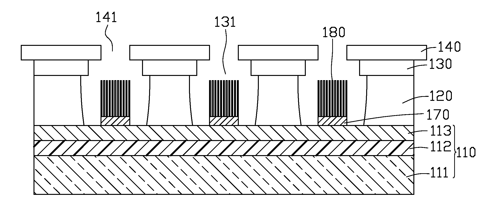
[0025]Reference will now be made to the drawings to describe a preferred embodiment of the present method for manufacturing a cathode assembly of a field emission display, in detail.

[0026]Referring to FIG. 1, a method for manufacturing a cathode assembly of a field emission display in accordance with a first preferred embodiment, includes the steps of:

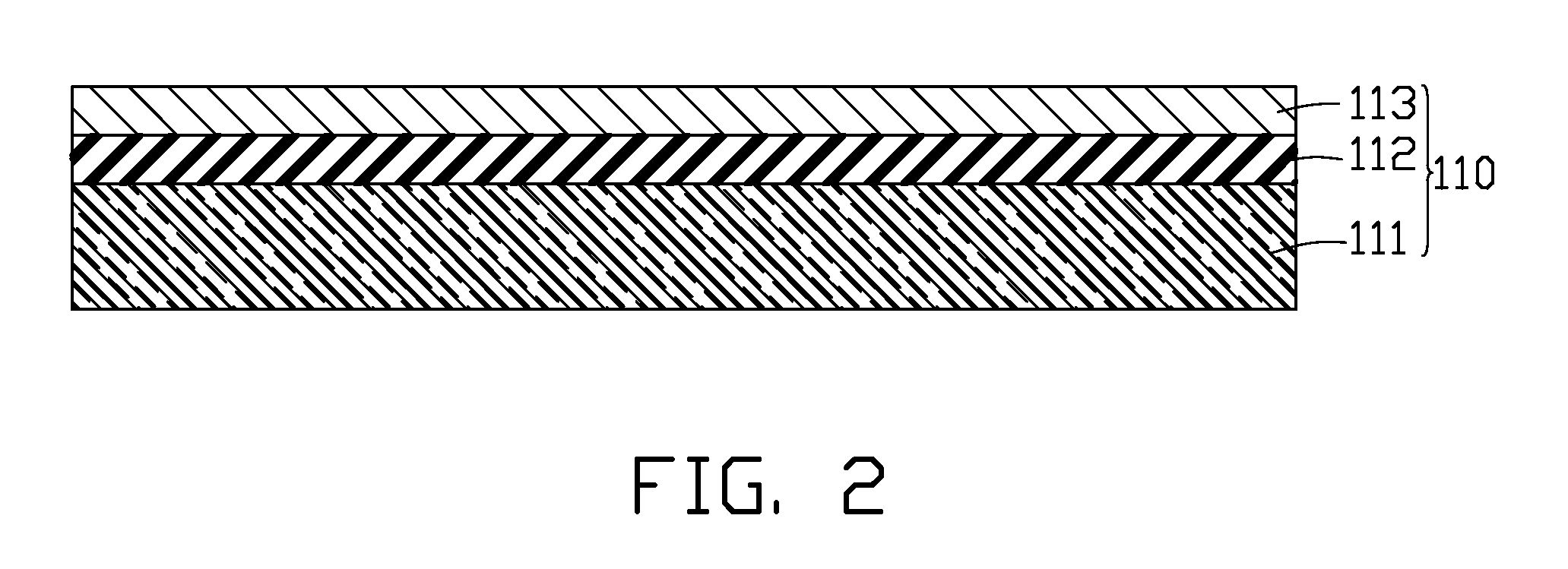
[0027]providing a substrate;

[0028]forming a cathode on the substrate;

[0029]forming an electrically insulating layer on the cathode;

[0030]forming a gate electrode layer on the first electrically insulating layer;

[0031]forming a photoresist layer on the gate electrode layer;

[0032]defining at least one opening in the photoresist layer using a photolithographic process;

[0033]etching the gate electrode layer through the at least one opening in the photoresist layer so as to form at least one gate electrode opening in the gate electrode layer;

[0034]etching the electrically insulating layer to define at least one cavity in the electrically in...


PUM


Abstract

A method for manufacturing a cathode assembly of a field emission display, includes the steps of: providing a substrate (110) with a cathode (113) formed thereon; forming an electrically insulating layer (120), a gate electrode layer (130) and a photoresist layer (140) on a cathode in series; defining at least one opening (141) in the photoresist layer using a photolithographic process; etching the gate electrode layer through the at least one opening so as to form at least one gate electrode opening (131) in the gate electrode layer; etching the electrically insulating layer to define at least one cavity (121) in the electrically insulating layer; pressing the photoresist layer in a manner such that a size of the at least one opening is reduced; depositing a catalyst layer (170) in the at least one cavity through the at least one opening; and growing carbon nanotubes (180) on the catalyst layer.

Description

CROSS REFERENCE TO RELATED APPLICATION[0001]This application is related to a commonly-assigned copending application Ser. No. 11 / 556,641, entitled “CARBON NANOTUBE FIELD EMISSION DEVICE AND METHOD FOR MANUFACTURING SAME”, filed Nov. 3, 2006.BACKGROUND OF THE INVENTION[0002]1. Field of the Invention[0003]The present invention relates to methods for manufacturing cathode assemblies of field emission displays and, more particularly, to a method for manufacturing a cathode assembly containing carbon nanotubes as electron emitters.[0004]2. Description of Related Art[0005]Field emission displays (FEDs) are a new, rapidly developing kind of flat panel display technology. Compared to conventional technologies, e.g., cathode-ray tube (CRT) and liquid crystal display (LCD) technologies, FEDs are superior in having a wider viewing angle, low energy consumption, smaller size, and higher quality display. In particular, carbon nanotube-based FEDs (CNTFEDs) have attracted much attention in recent ...

Claims


Application Information

Patent Timeline
Patent Type & Authority Patents(United States)
IPC IPC(8): H01L21/00
CPCB82Y10/00H01J9/025H01J29/86H01J31/127H01J2201/30469Y10S977/735Y10S977/742
Inventor ZHENG, ZHIFAN, SHOU-SHAN
Owner TSINGHUA UNIV
Why Eureka
Try Eureka