

Solid-state image pickup device and driving method therefor
- Summary
- Abstract
- Description
- Claims
- Application Information
AI Technical Summary
Benefits of technology
Problems solved by technology
Method used
Image

Examples
first example
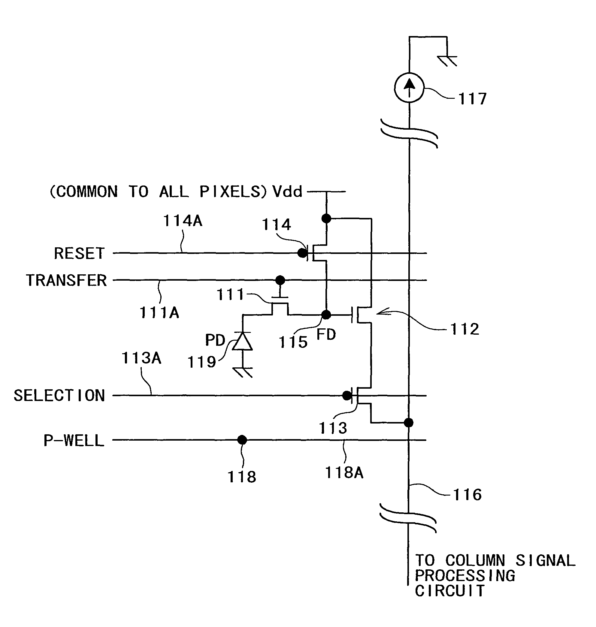
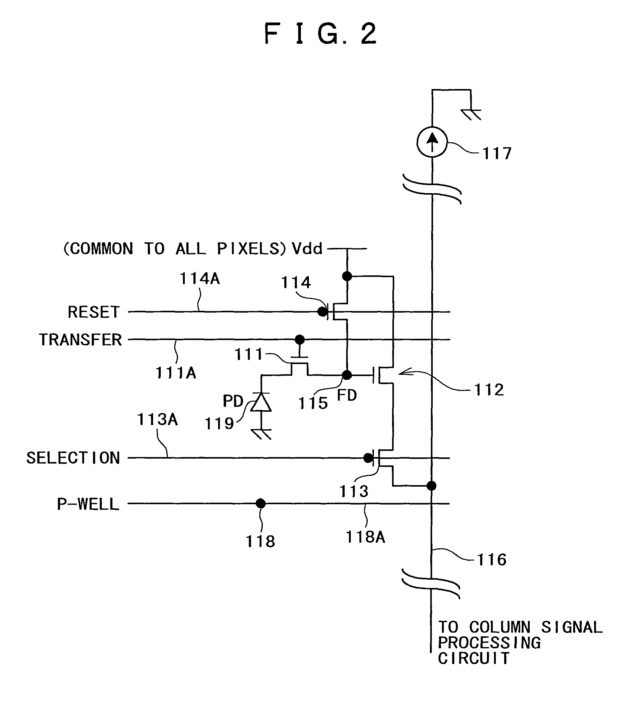
[0092]First, a particular example wherein a substrate bias is applied to the P-well regions below the pixel section described above is described as a first example.
[0093]FIG. 4 is a plan view showing a configuration of the P-well regions below the pixel section according to the first example. Referring to FIG. 4, P-well regions 200 are indicated by slanting lines, and a blank portion between such P-well regions 200 indicates a P-well isolation region 210. Further, a square region in each of the P-well regions 200 indicates one pixel 110A.
[0094]In short, in the configuration shown in FIG. 4, the P-well regions 200 are provided in an electrically isolated relationship from each other along the individual pixel rows of the pixel section 110.
[0095]FIG. 5 is a timing chart illustrating driving pulses applied to one of the pixel circuits in the first example.
[0096]Referring to FIG. 5, it is assumed that, as a prerequisite of the operation illustrated in the timing chart, the vertical sele...
second example
[0110]Now, an example wherein a substrate bias is applied to the P-well regions below the pixel section described above not in a unit of a row but over the overall pixel section is described as a second example.
[0111]FIG. 6 is a plan view showing a configuration of the P-well regions below the pixel section in the second example, and in FIG. 6, P-well regions 220 are indicated by slanting lines. In particular, in the present example, electrically conducting P-well regions 220 are provided over the overall area of the pixel section 110.
[0112]FIG. 7 is a timing chart illustrating driving pulses to be applied to a pixel circuit in the second example.
[0113]First, the pixels in all of the rows are rendered operative at the same time, and transfer of charge is performed next to resetting of the floating diffusions 115. In particular, a reset pulse is applied first to reset the floating diffusions 115. Thereafter, a transfer pulse is applied to transfer photoelectrons of the photodiodes 11...
third example
[0123]Now, an example wherein the bias voltage to each P-well region below the pixel section described above is varied intermediately within a charge storage period to expand the dynamic range is described as a third example.
[0124]FIG. 8 is a timing chart illustrating an example of operation where the bias voltage to a P-well region is varied intermediately within a charge storage period, and the axis of ordinate indicates the P-well voltage and the axis of abscissa indicates lapse of time. Meanwhile, FIG. 9 is a diagram illustrating a relationship between the amount of received light and the number of stored electrons of a photodiode in the operation illustrated in FIG. 8.
[0125]When storage of photoelectrons into a photodiode is started, the P-well voltage is set to, for example, −1 V as seen in FIG. 8. If the P-well voltage is changed to 0 V intermediately within the storage period, then, as seen in FIG. 9, where the light amount is small, the number of stored electrons into the p...
PUM
 Abstract
Description
Claims
Application Information